Reparación fuente alimentación ATX Litepower 600
- informática
Reparación fuente alimentación ATX Litepower 600
Sección titulada «Reparación fuente alimentación ATX Litepower 600»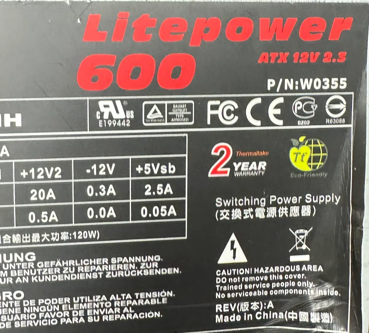
STPS30L45CT
Sección titulada «STPS30L45CT»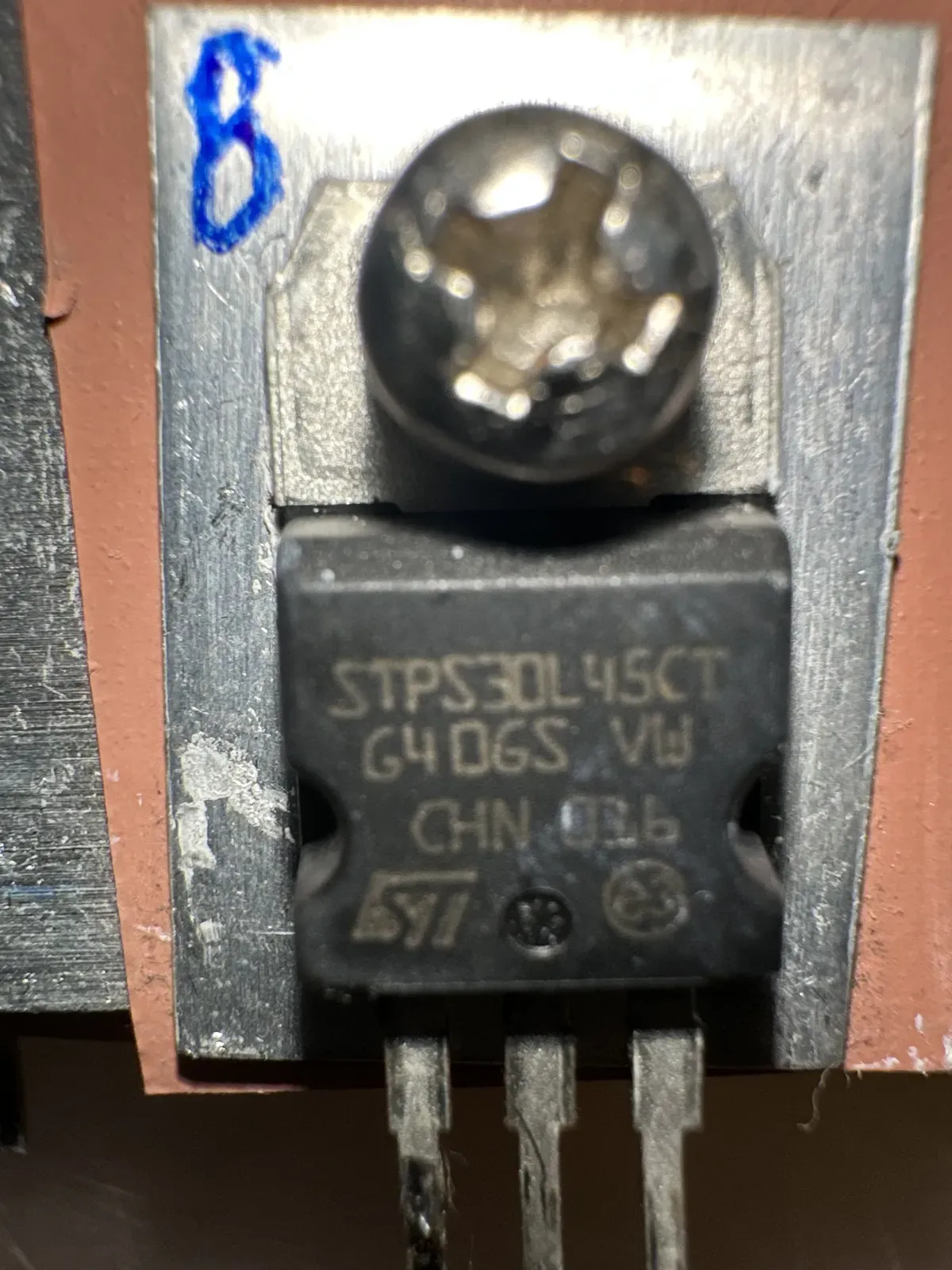
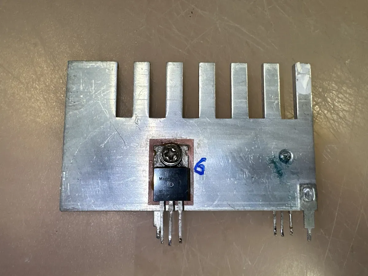
STPS30L45CT
Sección titulada «STPS30L45CT»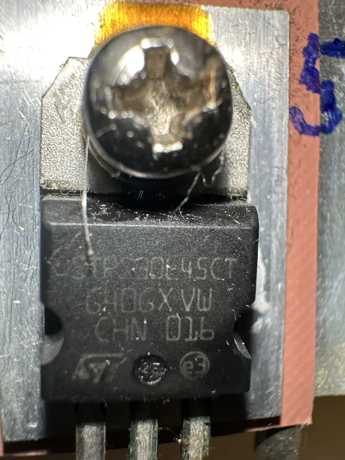
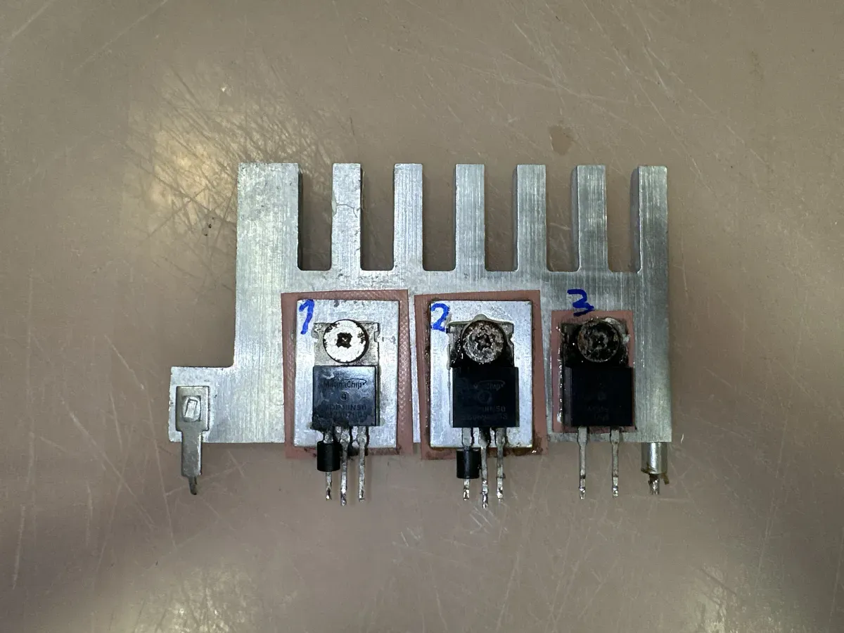
MDP18N50
Sección titulada «MDP18N50»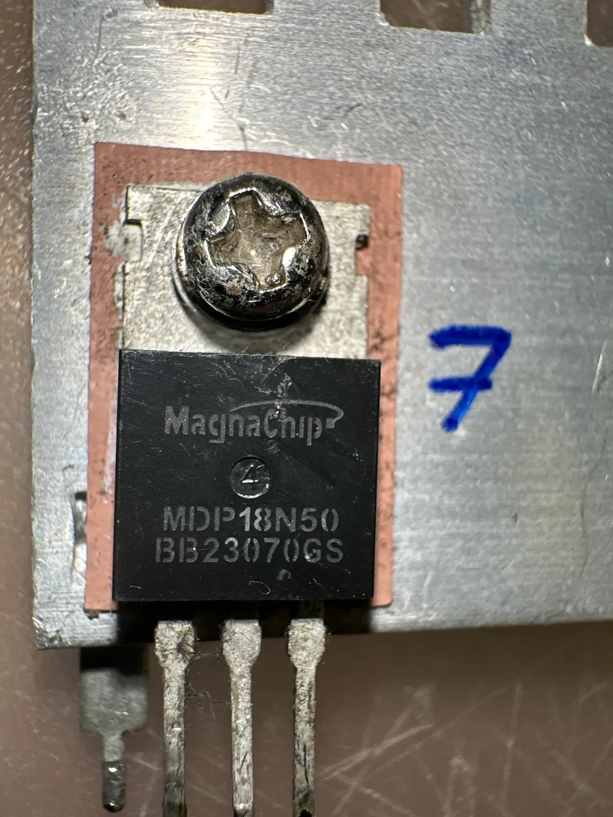
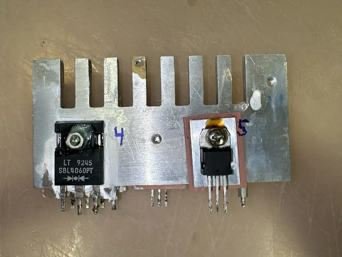
STPS30L45CT
Sección titulada «STPS30L45CT»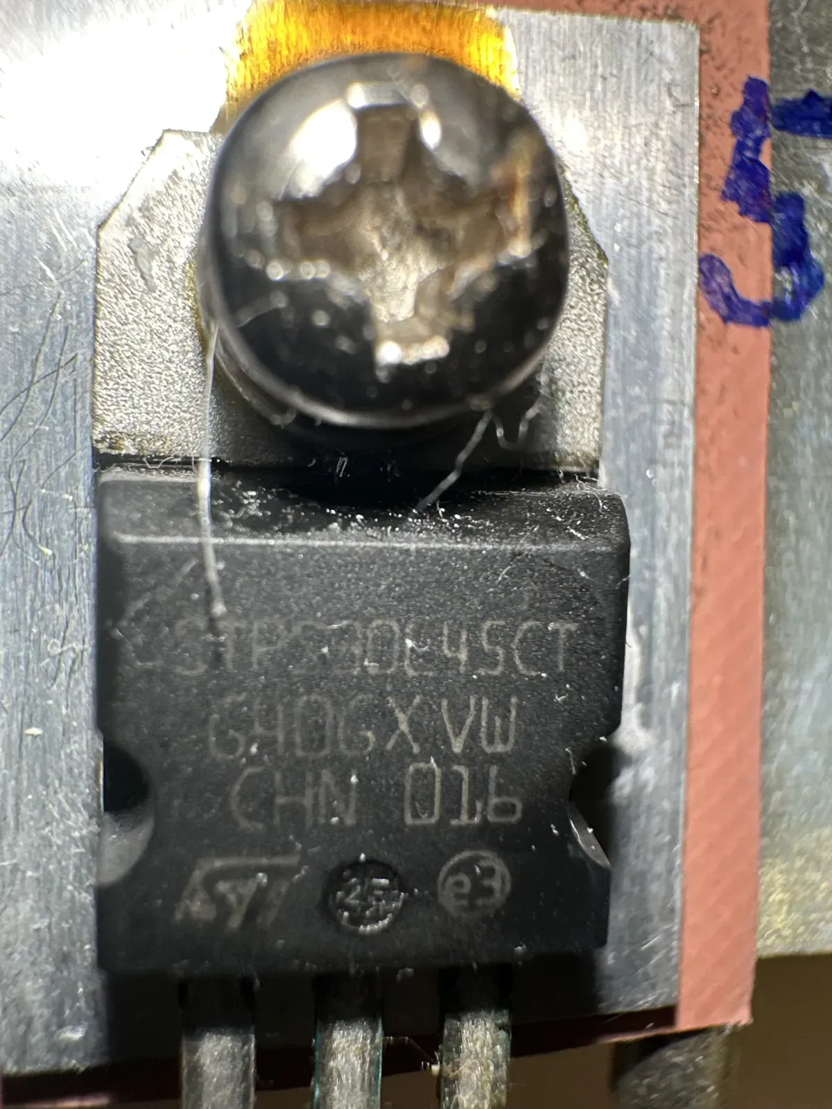
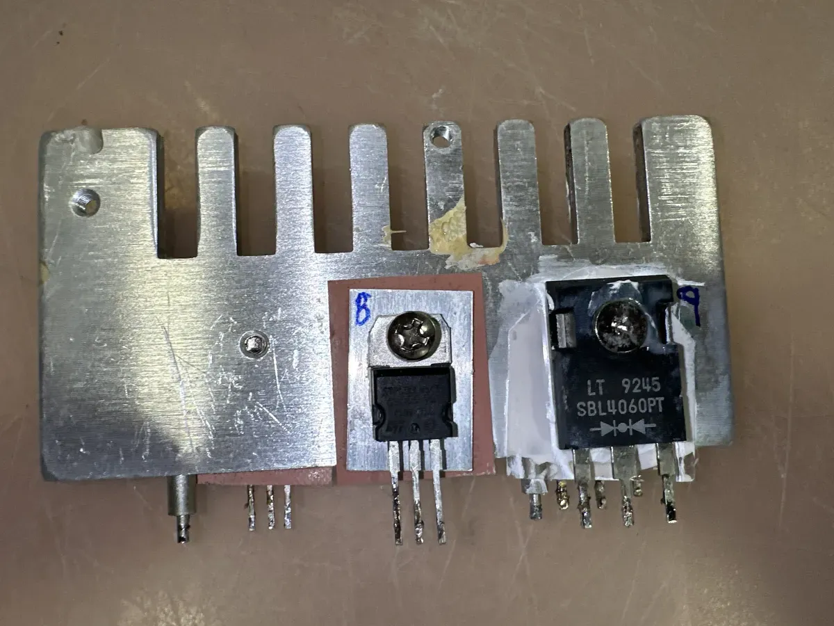
SBL4060PT
Sección titulada «SBL4060PT»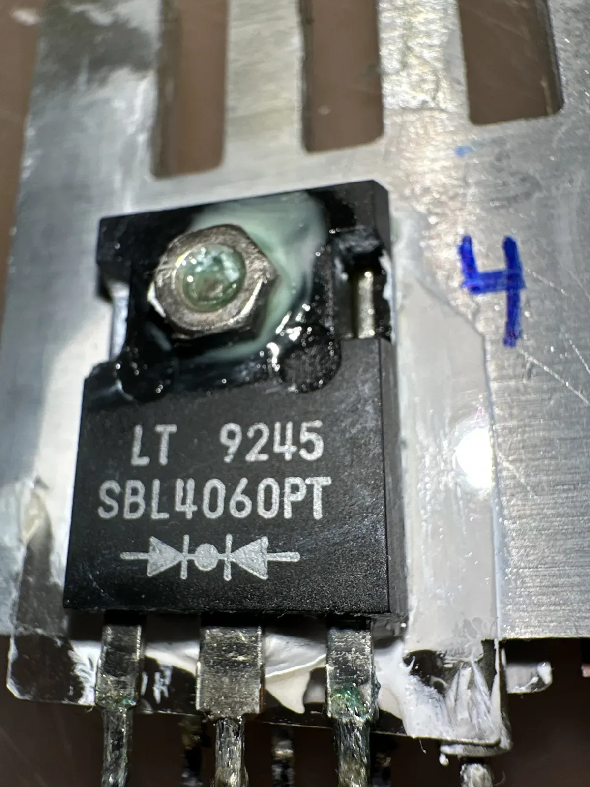
BYC10 600 - PJA1018 C5
Sección titulada «BYC10 600 - PJA1018 C5»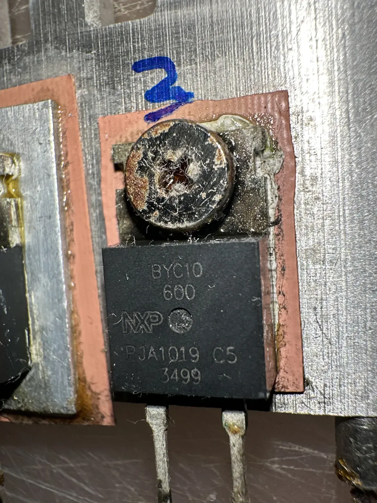
MDP18N50
Sección titulada «MDP18N50»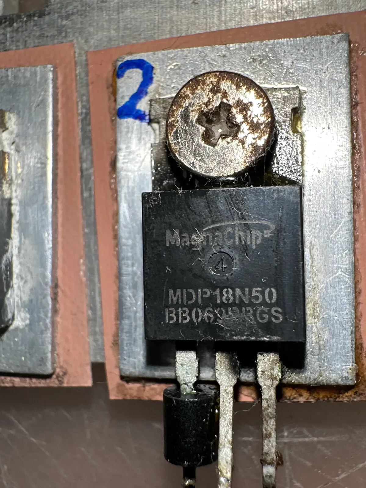
MDP18N50
Sección titulada «MDP18N50»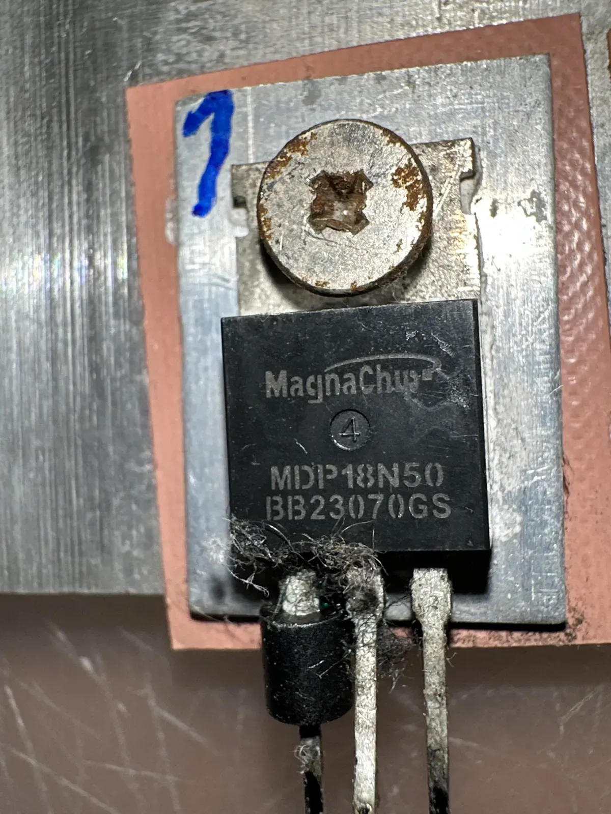
MDP18N50
Sección titulada «MDP18N50»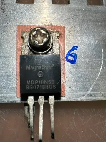
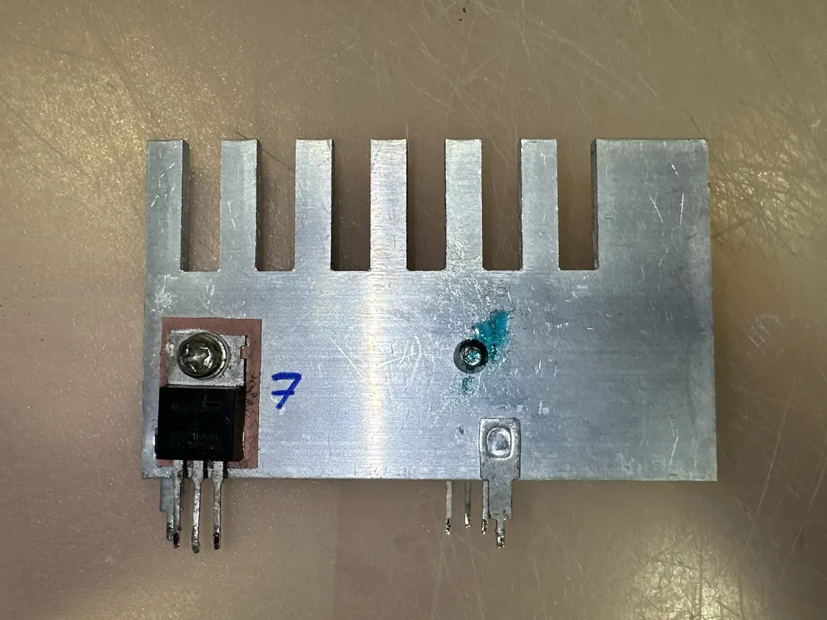
CM6800G
Sección titulada «CM6800G»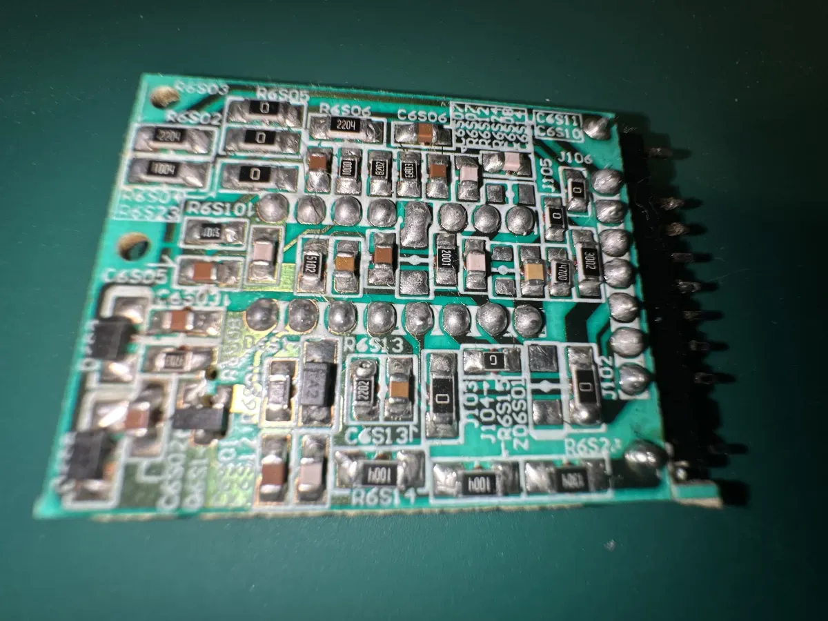
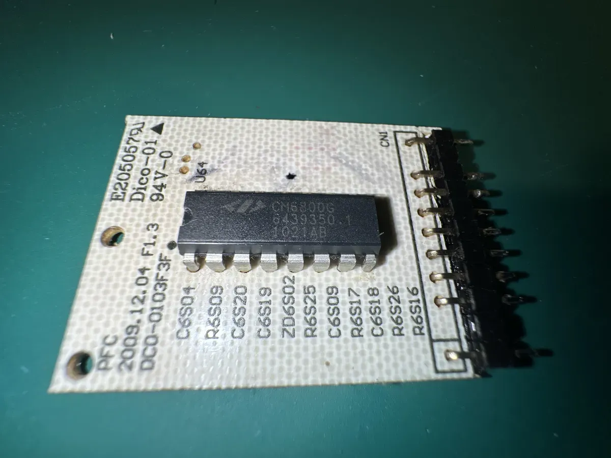
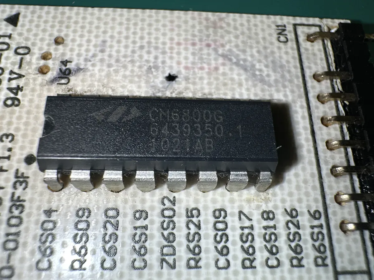
CM6800G
The CM6800 is a controller for power factor corrected, switched mode power suppliers. Power Factor Correction (PFC) allows the use of smaller, lower cost bulk capacitors, reduces power line loading and stress on the switching FETs, and results in a power supply that fully compiles with IEC-1000-3-2 specifications. Intended as a BiCMOS version of the industry-standard ML4824,
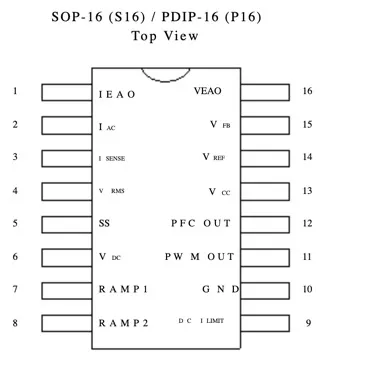
The CM6800 is an integrated circuit (IC) that combines Power Factor Correction (PFC) and Pulse Width Modulation (PWM) control into a single chip.
Key Features & Overview
• Function: Controls switched-mode power supplies (SMPS) by integrating a leading-edge average current PFC controller and a trailing-edge PWM controller. • Compatibility: Pin-compatible with industry-standard controllers like the ML4800 and FAN4800 families. • Package: Typically housed in a 16-pin SOP (Small Outline Package) or PDIP (Plastic Dual In-Line Package). • Common Applications: Used extensively in desktop PC ATX power supplies, server and IPC power supplies, uninterruptible power supplies (UPS), and battery chargers. • Core Benefits: Improves power factor to reduce energy waste, allows for smaller bulk capacitors, and features low start-up/operating c
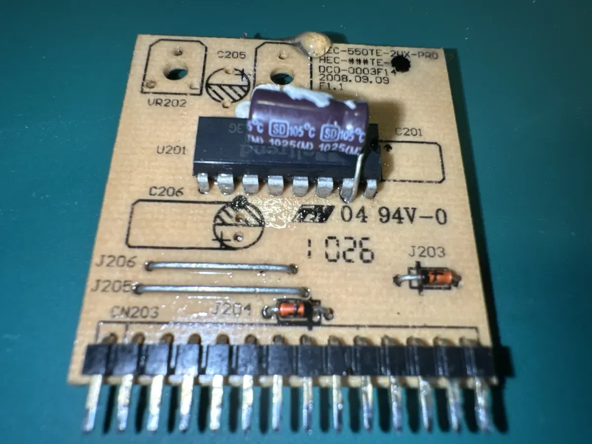
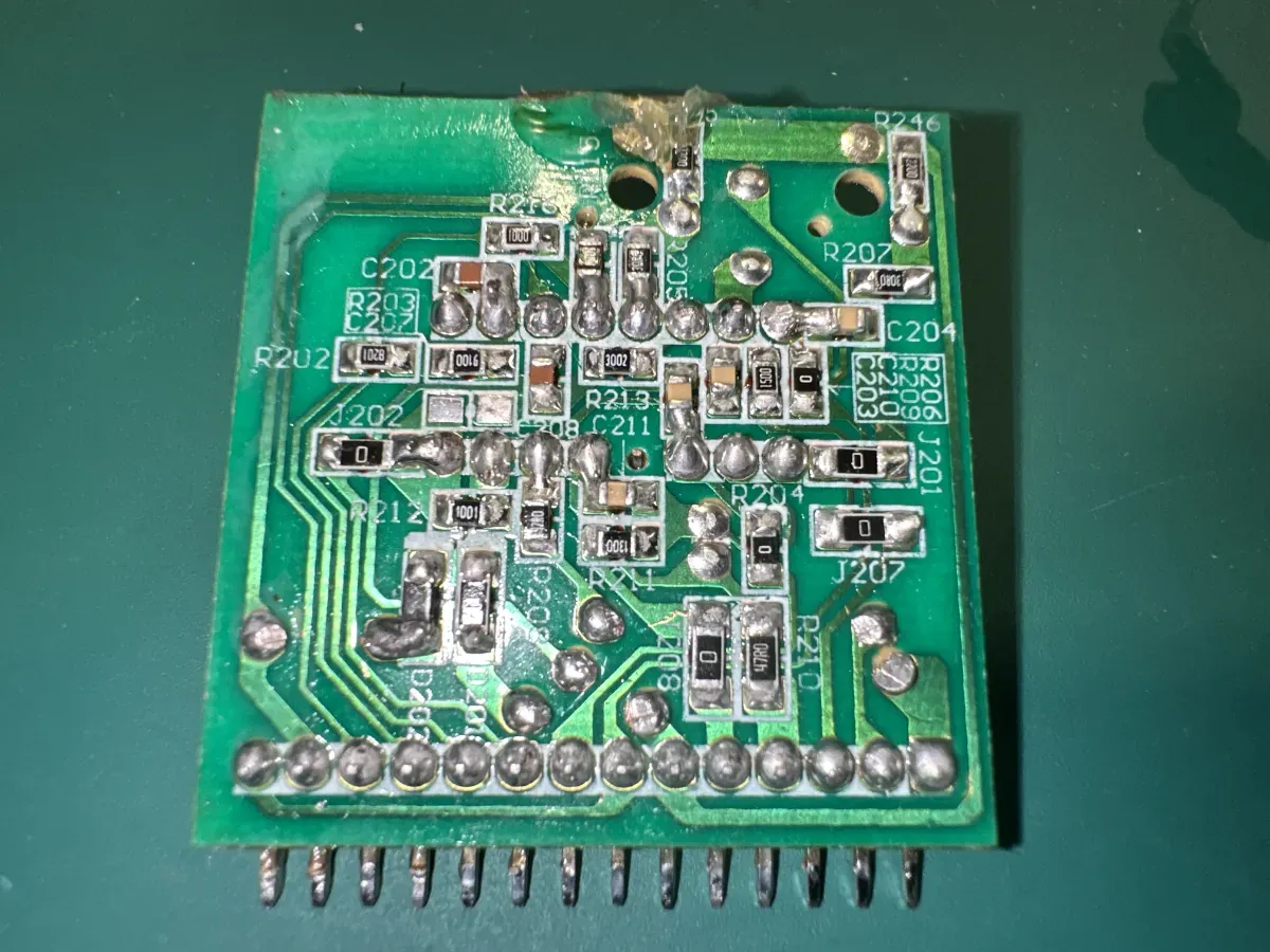
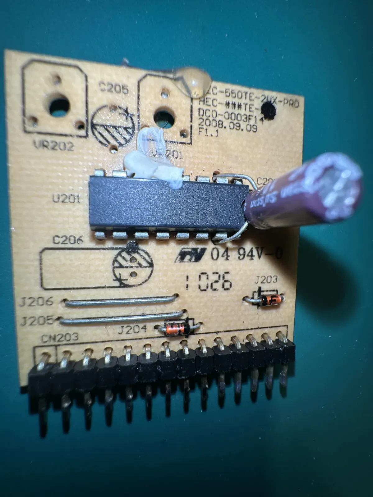
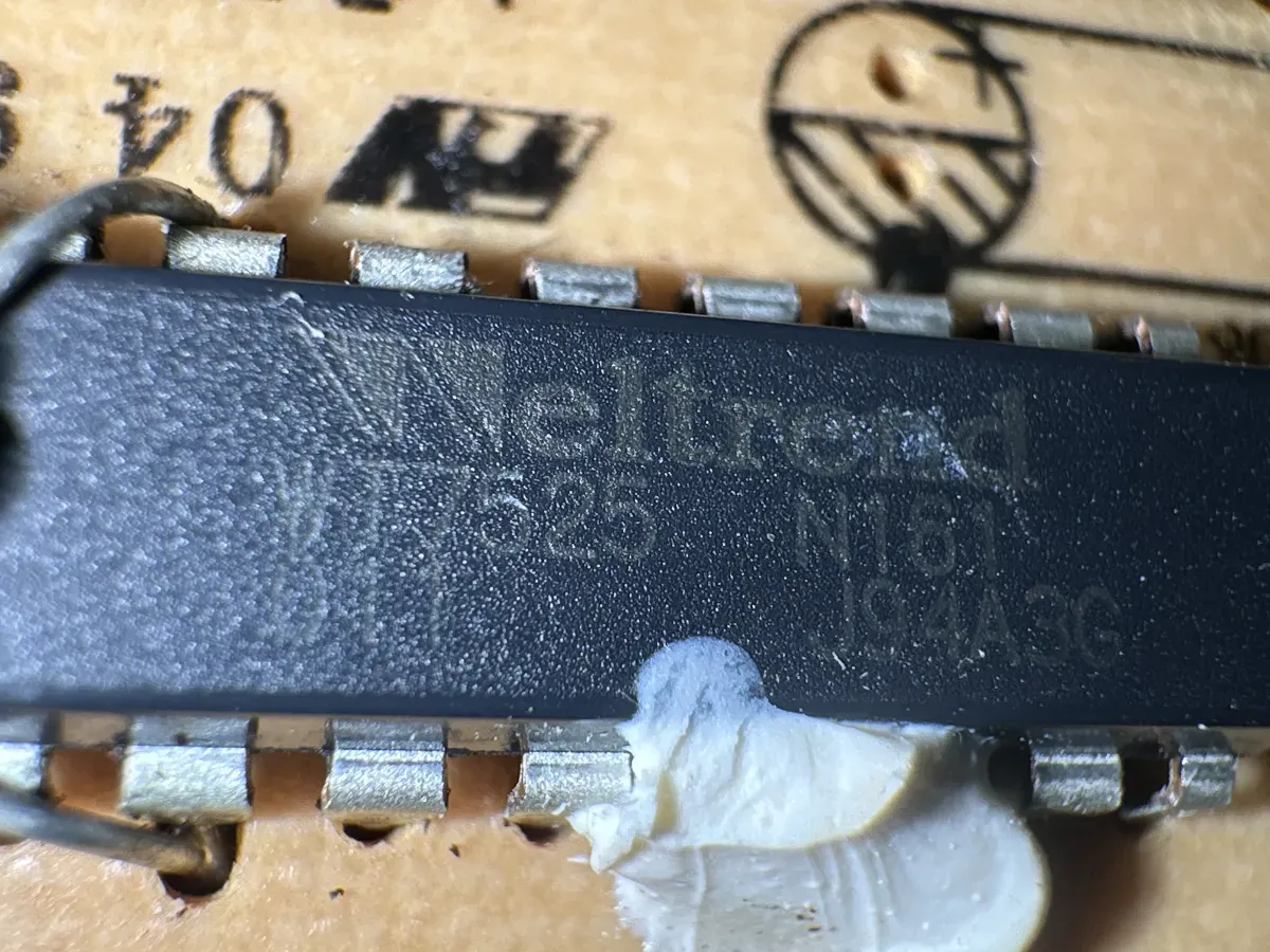
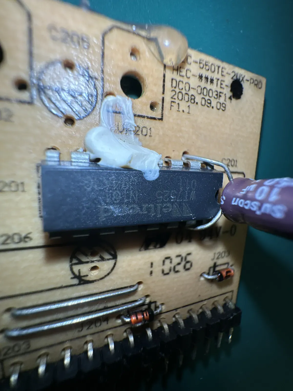
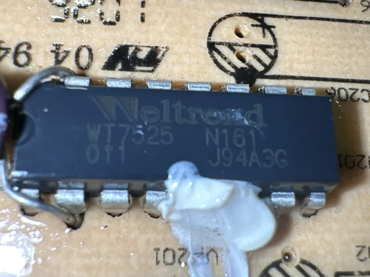
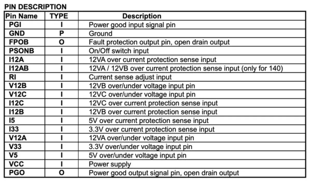
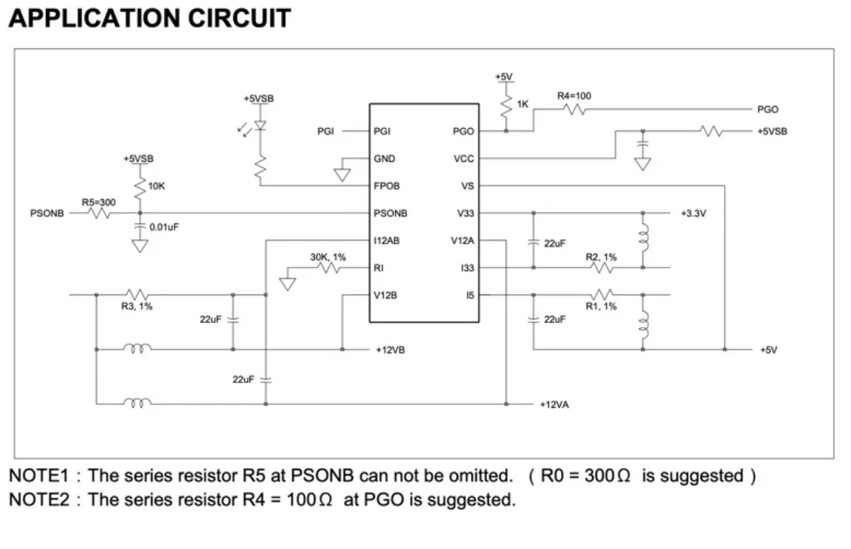
The WT7525 provides protection circuits, power good output (PGO), fault protection latch (FPOB), and a protection detector function (PSONB) control. It can minimize external components of switching power supply systems in personal computer. The Over / Under Voltage Detector (OVD / UVD) monitors V33, V5, V12A, V12B and V12C input voltage level. The Over Current Detector (OCD) monitor IS33, IS5, IS12A, IS12B and IS12C input current sense. When OVD or UVD or OCD detect the fault voltage level, the FPOB is latched HIGH and PGO go low. The latch can be reset by PSONB go HIGH. There is 3.5 ms delay time for PSONB turn off FPOB. When OVD and UVD and OCD detect the right voltage level, the power good output (PGO) will be issue. FEATURES · The Over/Under Voltage Detector (OVD / UVD) monitors V33, V5, V12A, V12B and V12C input voltage. · The Over Current Detector (OCD) monitors IS33, IS5, IS12A, IS12B and IS12C input current sense. · Both of the power good output (PGO) and fault protection latch (FPOB) are Open Drain Output. · 75 / 300 ms time delay for UVD. · 300 ms time delay for PGO. · 38 ms for PSONB input signal De–bounce. · 73 us for PGI/OVD/UVD internal signal De–glitches. · 1.2 ms for OCD internal signal De–glitches. · 3.5 ms time delay for PSONB turn-off FPOB.
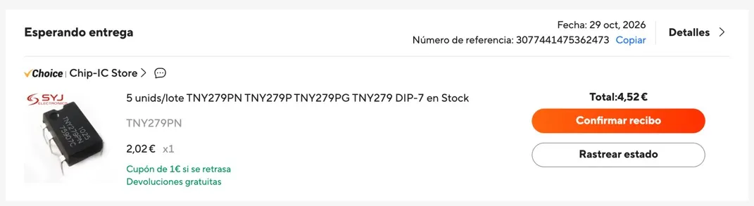
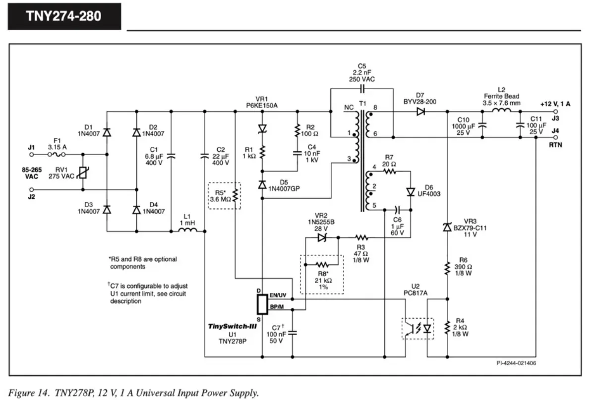
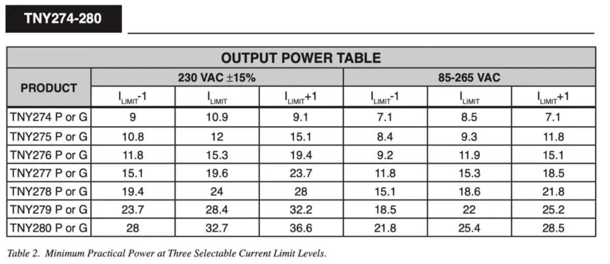
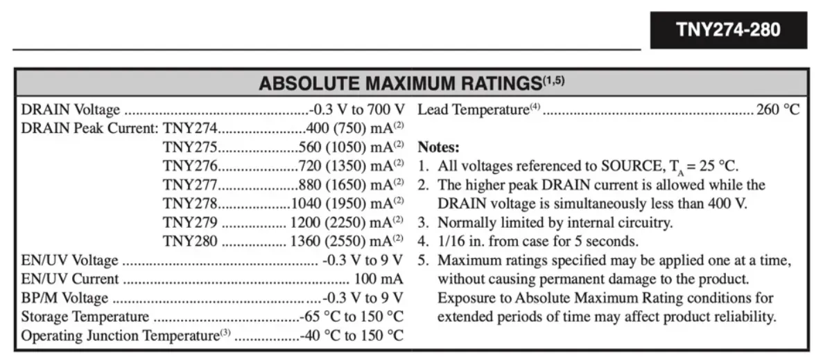
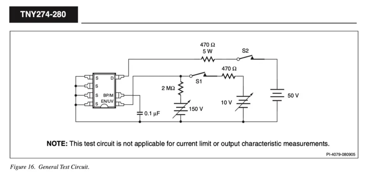
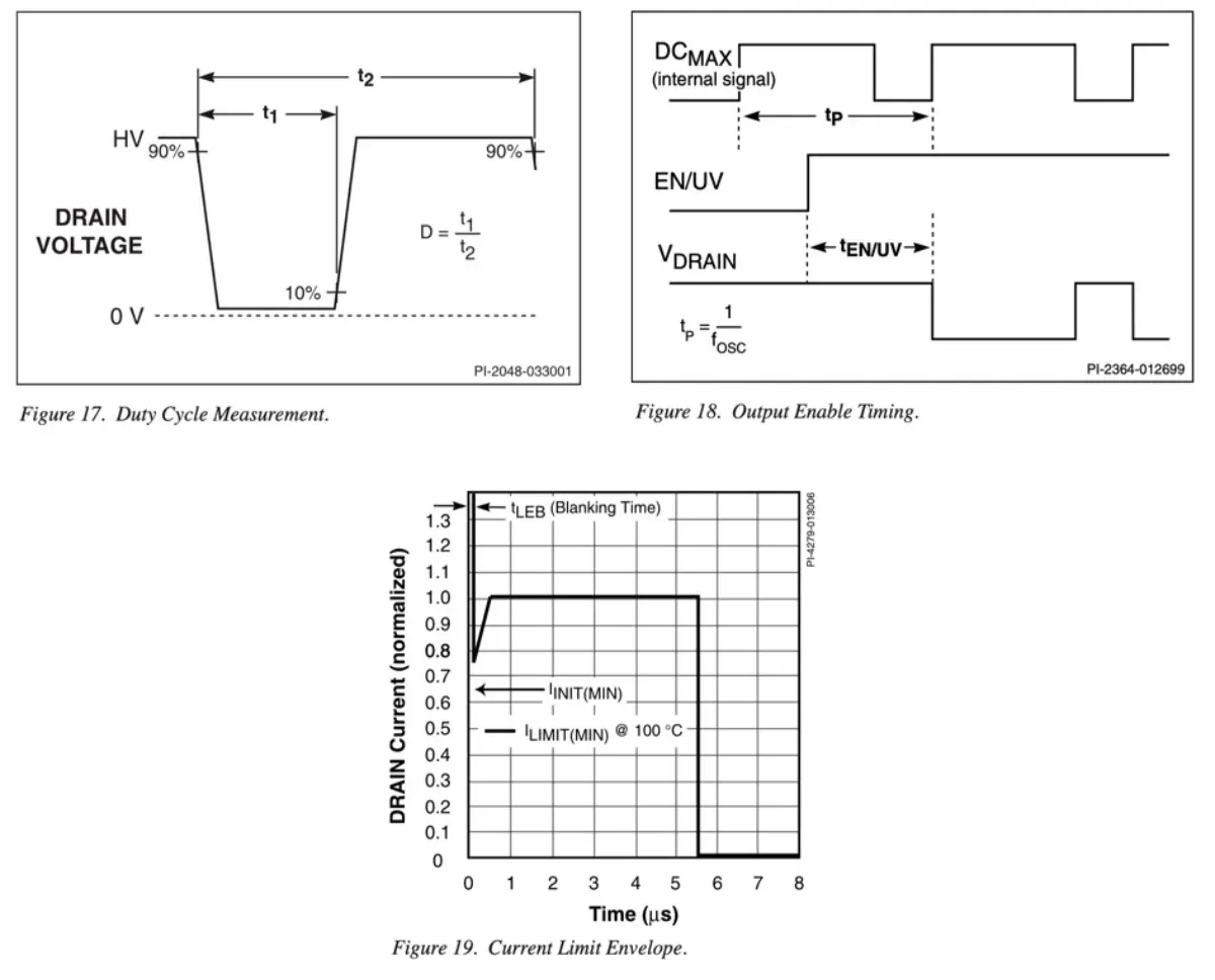
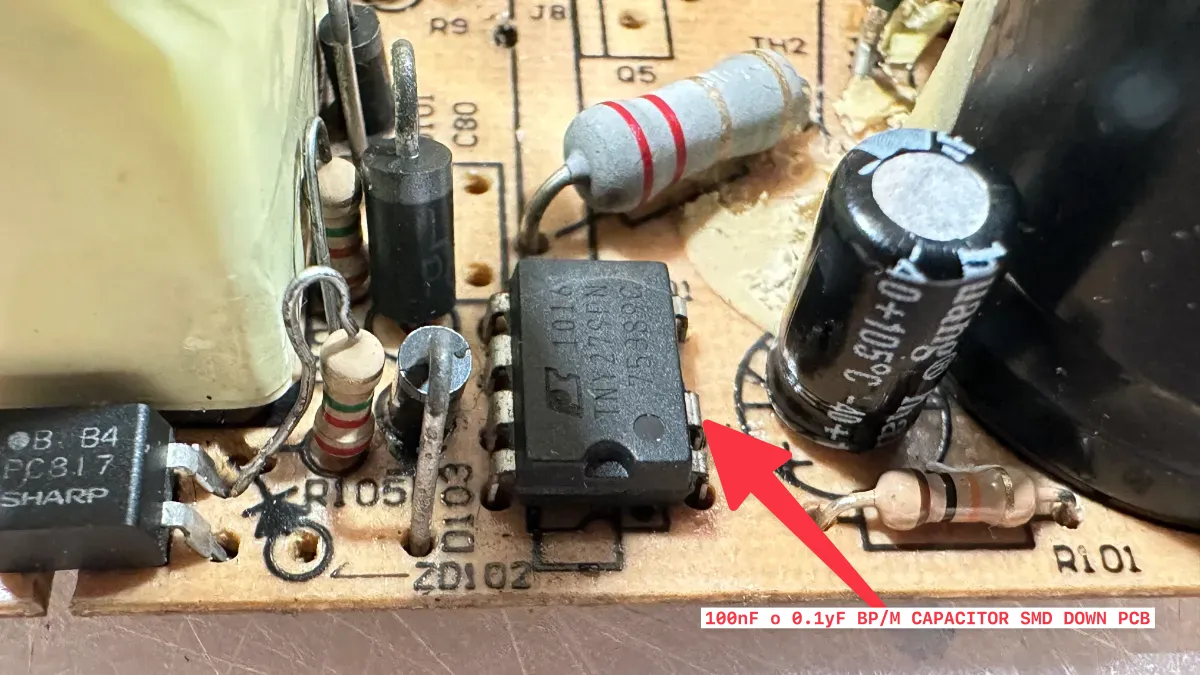
TNY279PN
Sección titulada «TNY279PN»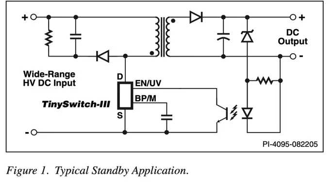
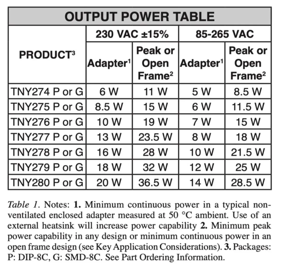
Lowest System Cost with Enhanced Flexibility • Simple ON/OFF control, no loop compensation needed • Selectable current limit through BP/M capacitor value
- Higher current limit extends peak power or, in open frame applications, maximum continuous power
- Lower current limit improves efficiency in enclosed adapters/chargers
- Allows optimum TinySwitch-III choice by swapping devices with no other circuit redesign • Tight I2f parameter tolerance reduces system cost
- Maximizes MOSFET and magnetics power delivery
- Minimizes max overload power, reducing cost of transformer, primary clamp & secondary components • ON-time extension – extends low line regulation range/ hold-up time to reduce input bulk capacitance • Self-biased: no bias winding or bias components • Frequency jittering reduces EMI filter costs • Pin-out simplifies heatsinking to the PCB • SOURCE pins are electrically quiet for low EMI Enhanced Safety and Reliability Features • Accurate hysteretic thermal shutdown protection with automatic recovery eliminates need for manual reset • Improved auto-restart delivers <3% of maximum power in short circuit and open loop fault conditions • Output overvoltage shutdown with optional Zener • Line under-voltage detect threshold set using a single optional resistor • Very low component count enhances reliability and enables single-sided printed circuit board layout • High bandwidth provides fast turn on with no overshoot and excellent transient load response • Extended creepage between DRAIN and all other pins improves field reliability EcoSmart®– Extremely Energy Efficient • Easily meets all global energy efficiency regulations • No-load <150 mW at 265 VAC without bias winding, <50 mW with bias winding • ON/OFF control provides constant efficiency down to very light loads – ideal for mandatory CEC regulations and 1 W PC standby requirements
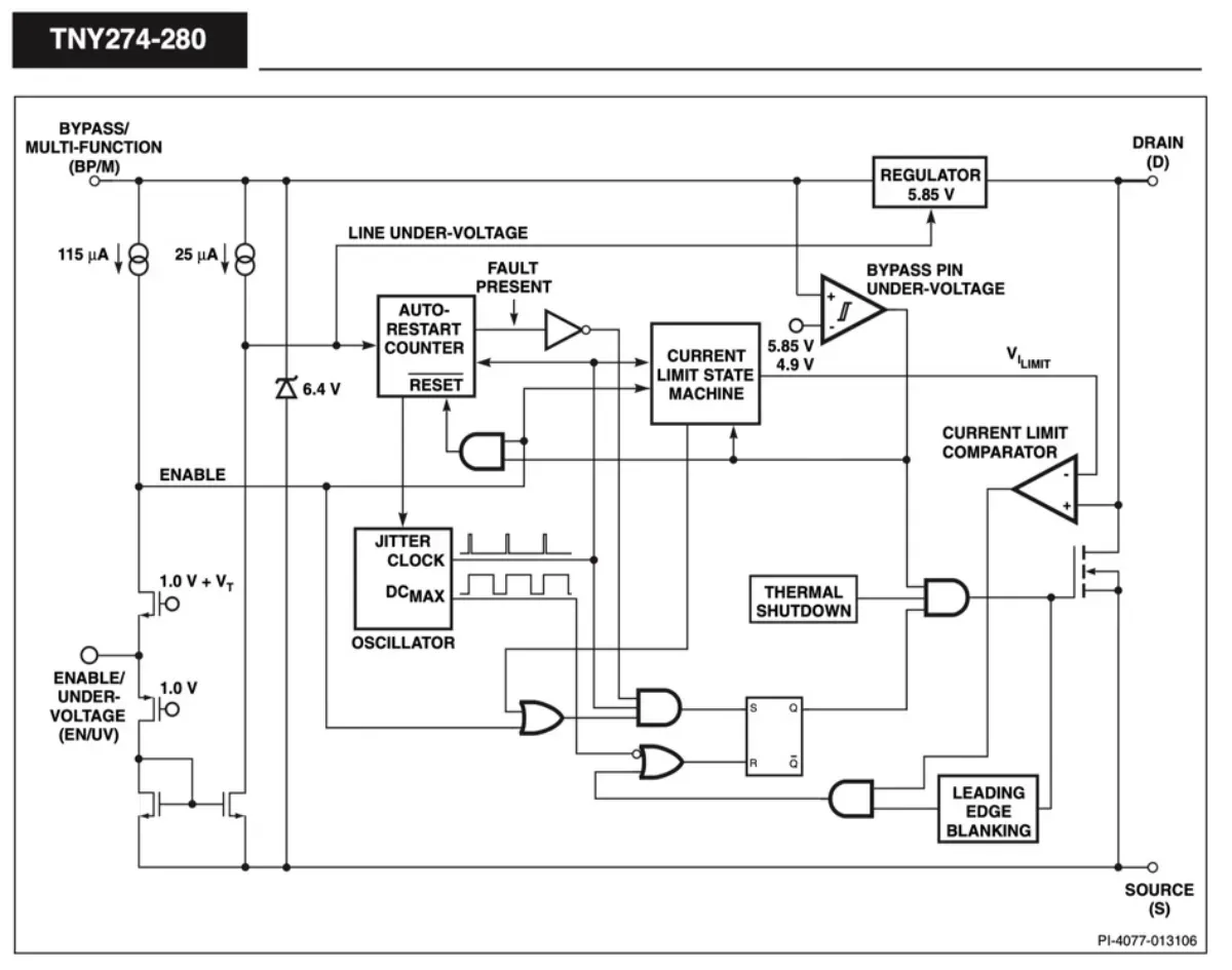
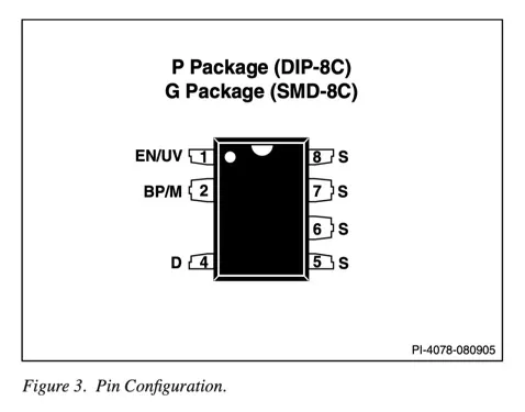
Pin Functional Description
DRAIN (D) Pin:
This pin is the power MOSFET drain connection. It provides
internal operating current for both start-up and steady-state
operation.
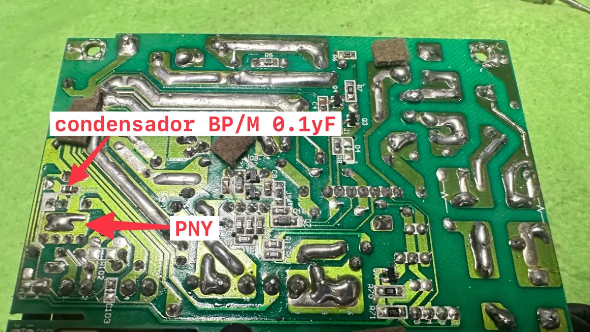
BYPASS/MULTI-FUNCTION (BP/M) Pin:
This pin has multiple functions:
3. It is the connection point for an external bypass capacitor
for the internally generated 5.85 V supply.
It is a mode selector for the current limit value, depending
on the value of the capacitance added. Use of a 0.1 µF
capacitor results in the standard current limit value. Use of
a 1 µF capacitor results in the current limit being reduced to
that of the next smaller device size. Use of a 10 µF capacitor
results in the current limit being increased to that of the next
larger device size for TNY275-280.
It provides a shutdown function. When the current into the
bypass pin exceeds 5.5 mA, the device latches off until the
BP/M voltage drops below 4.9 V, during a power down.
This can be used to provide an output overvoltage function
with a Zener connected from the BP/M pin to a bias winding
supply.
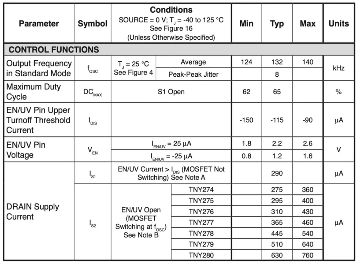
ENABLE/UNDER-VOLTAGE (EN/UV) Pin:
This pin has dual functions: enable input and line under-voltage
sense. During normal operation, switching of the power
MOSFET is controlled by this pin. MOSFET switching is
terminated when a current greater than a threshold current is
drawn from this pin. Switching resumes when the current being
pulled from the pin drops to less than a threshold current. A
modulation of the threshold current reduces group pulsing. The
threshold current is between 60 µA and 115 µA.
The EN/UV pin also senses line under-voltage conditions through
an external resistor connected to the DC line voltage. If there is
no external resistor connected to this pin, TinySwitch-III detects
its absence and disables the line under-voltage function.
SOURCE (S) Pin:
This pin is internally connected to the output MOSFET source
for high voltage power return and control circuit common.
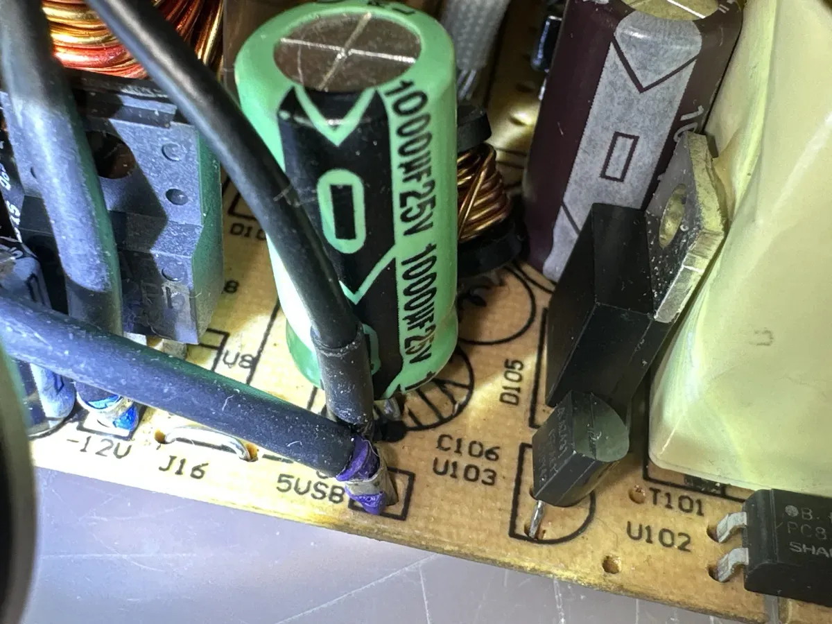
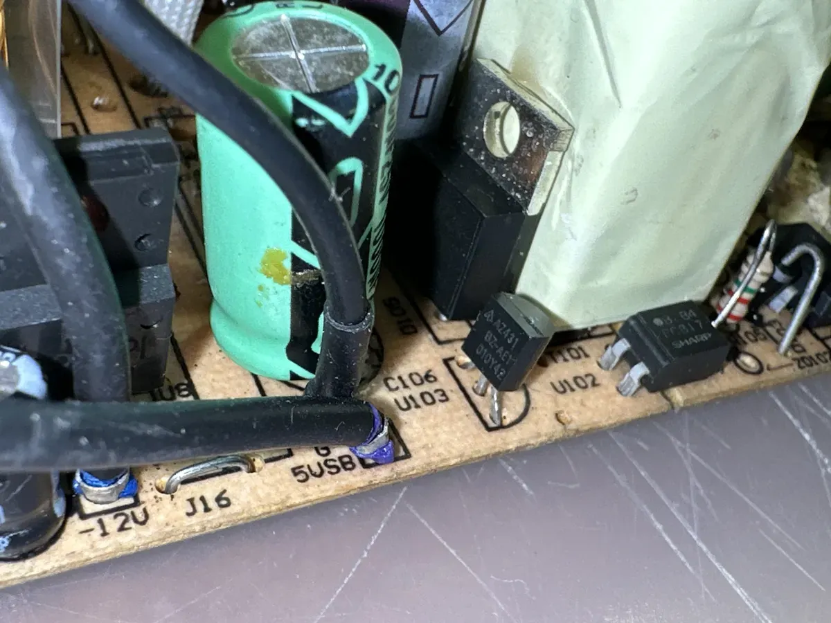
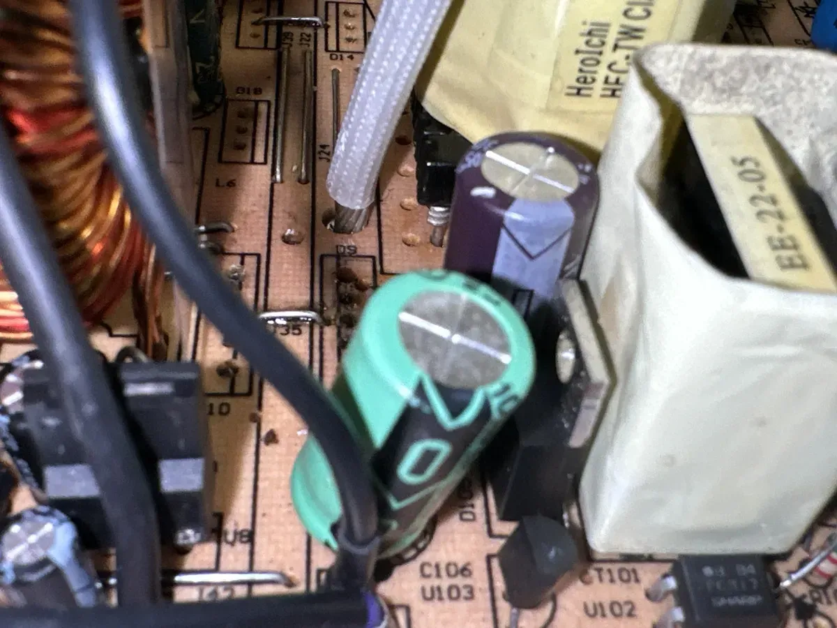
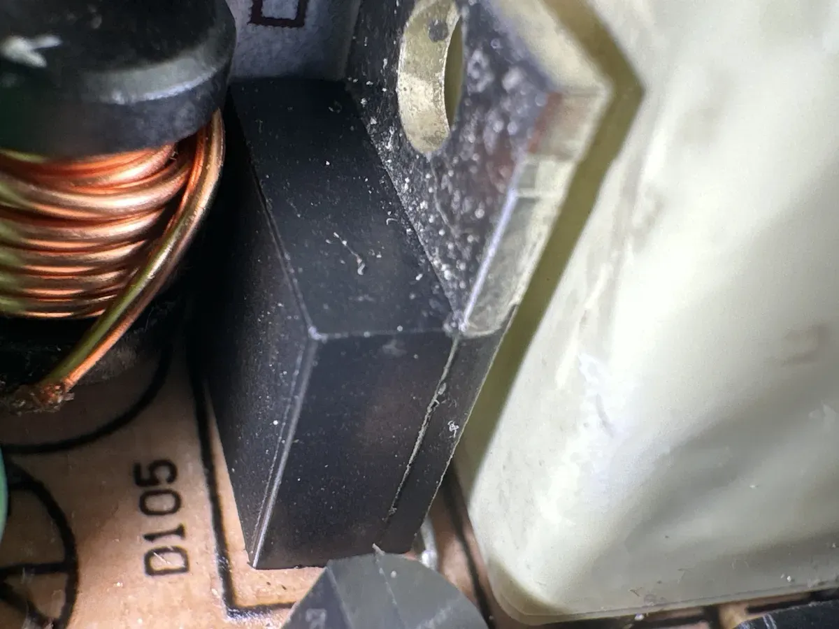
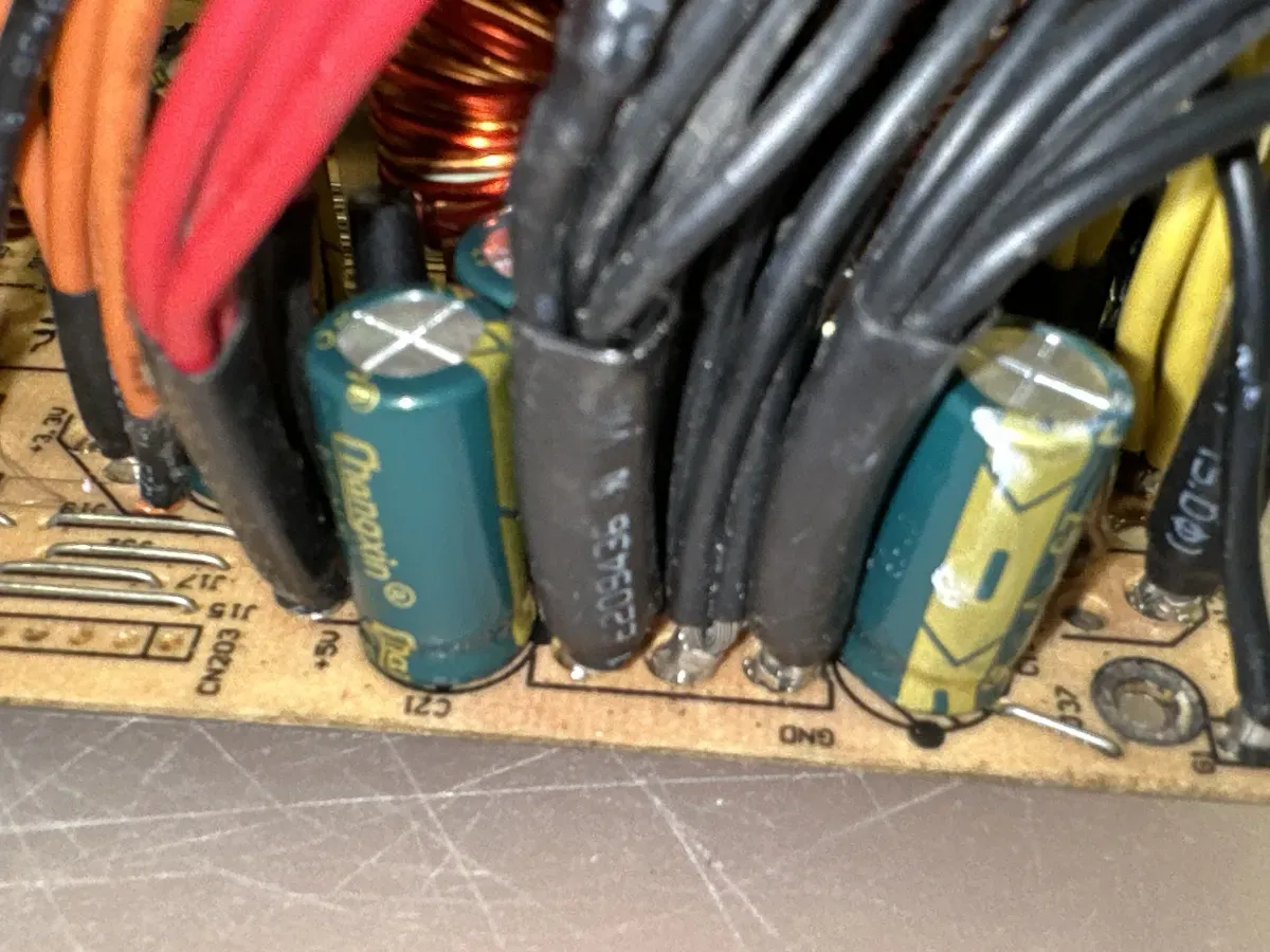
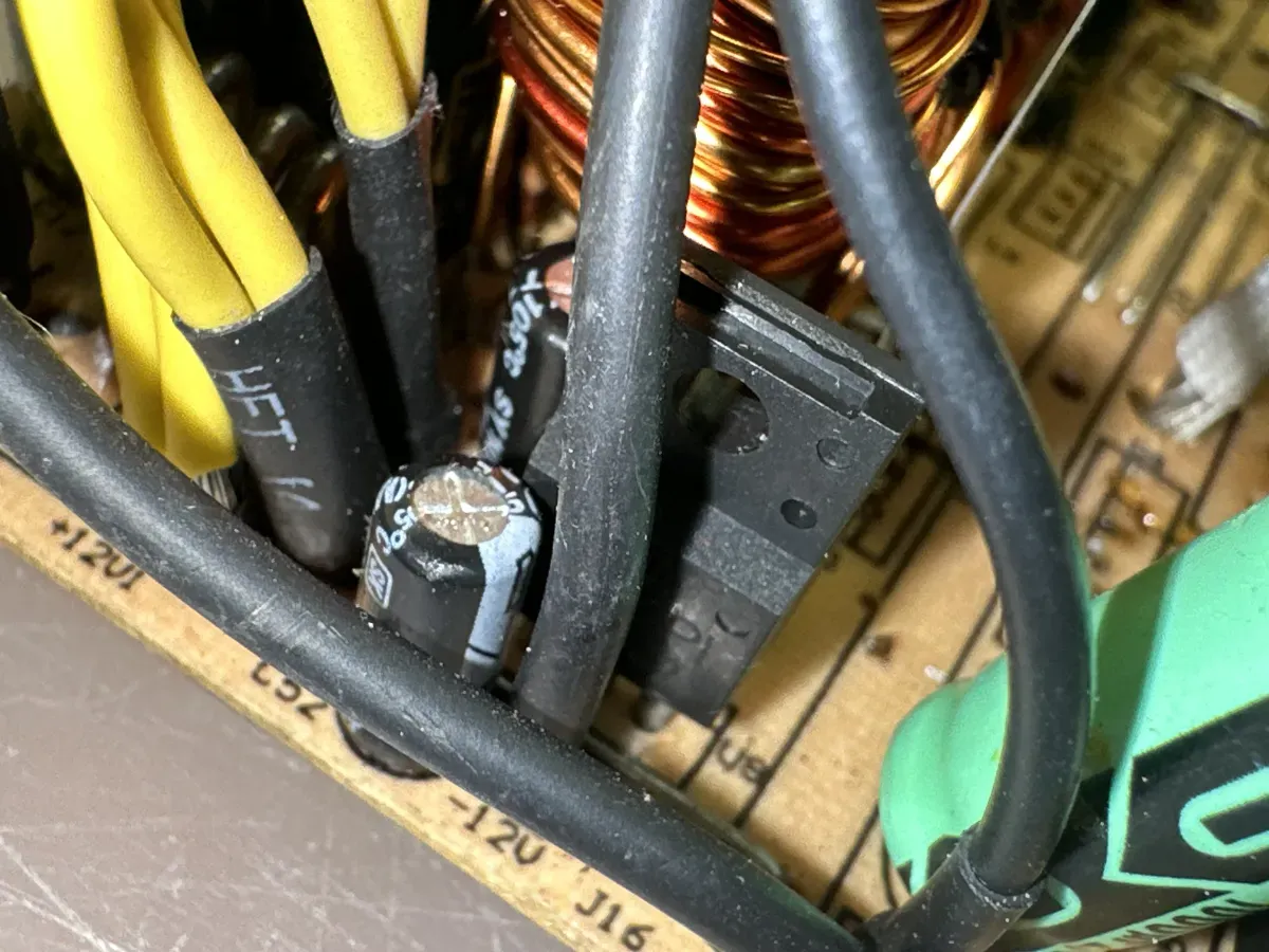
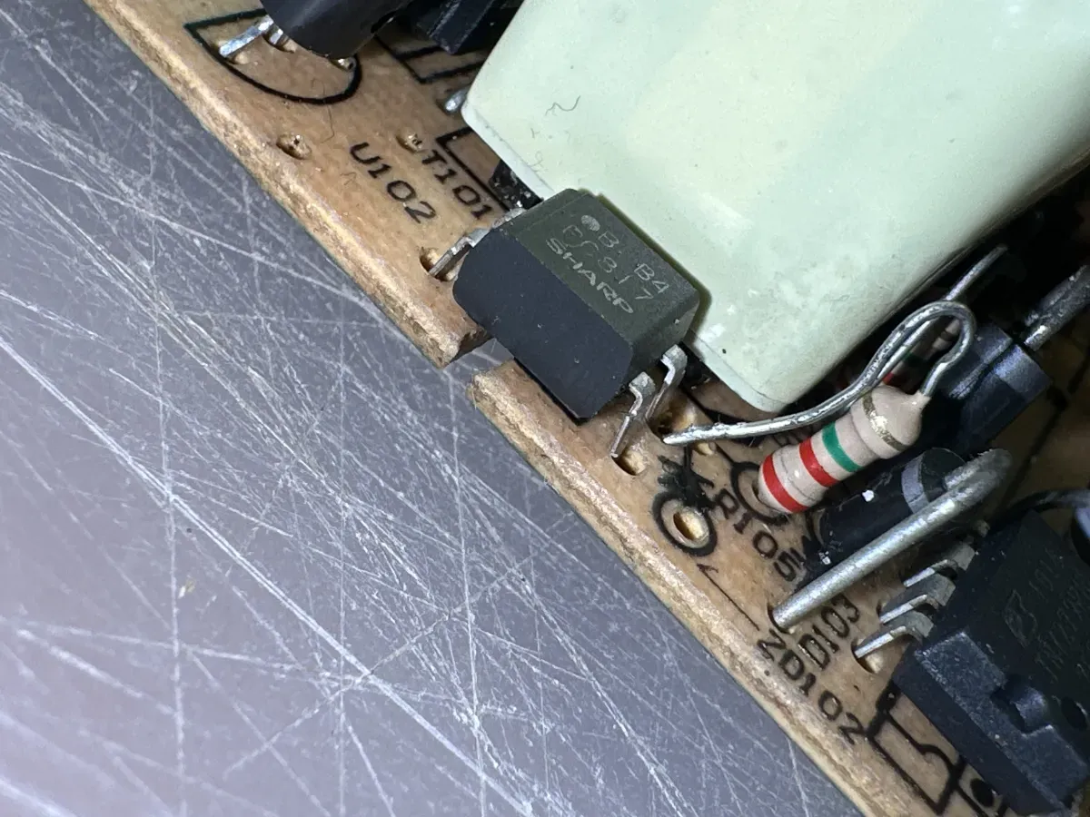
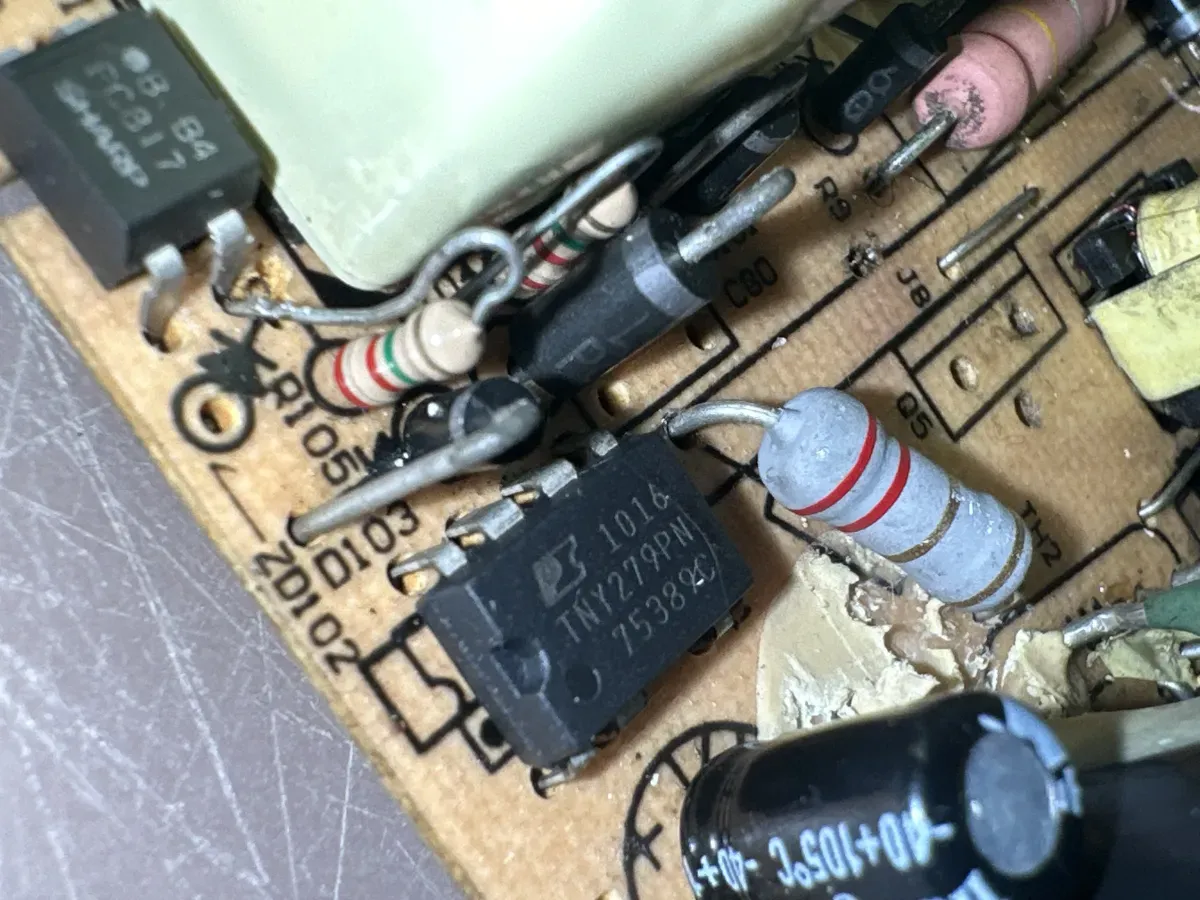
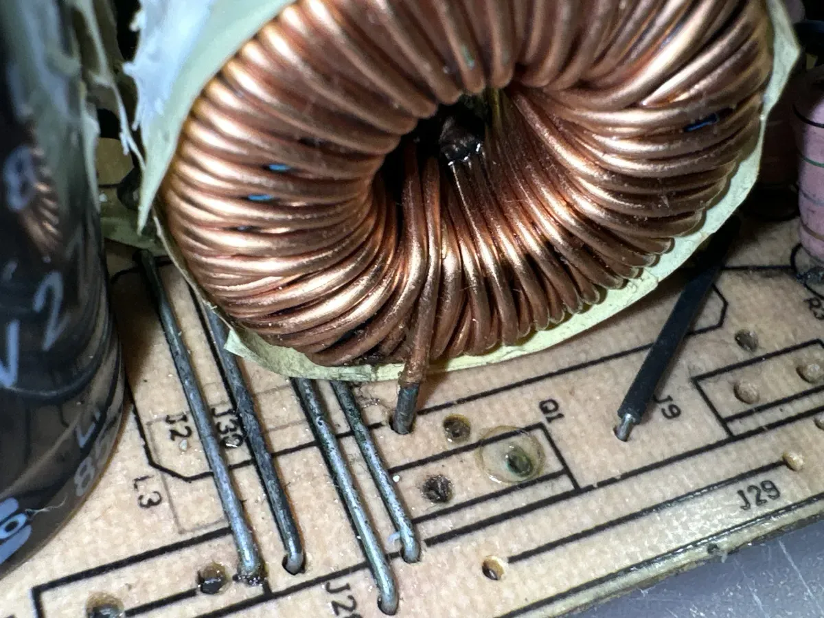
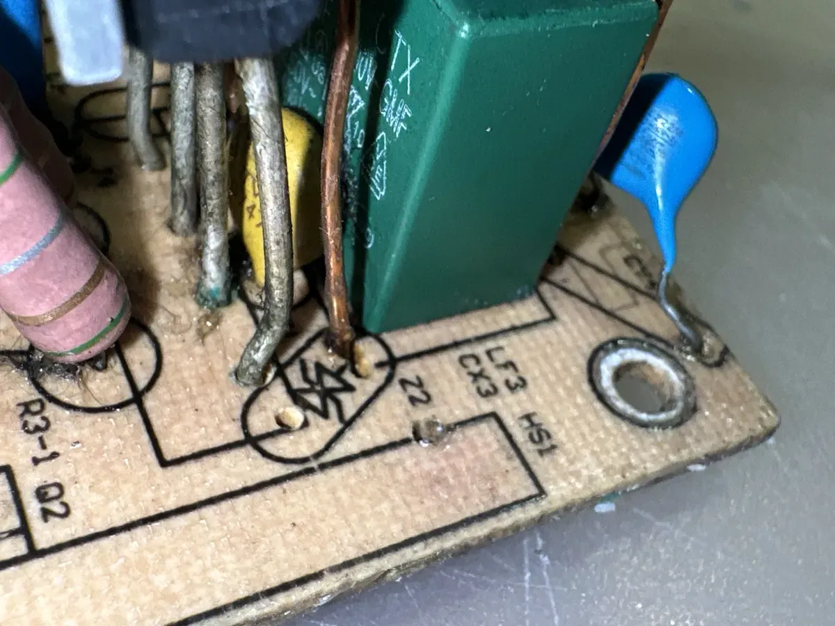
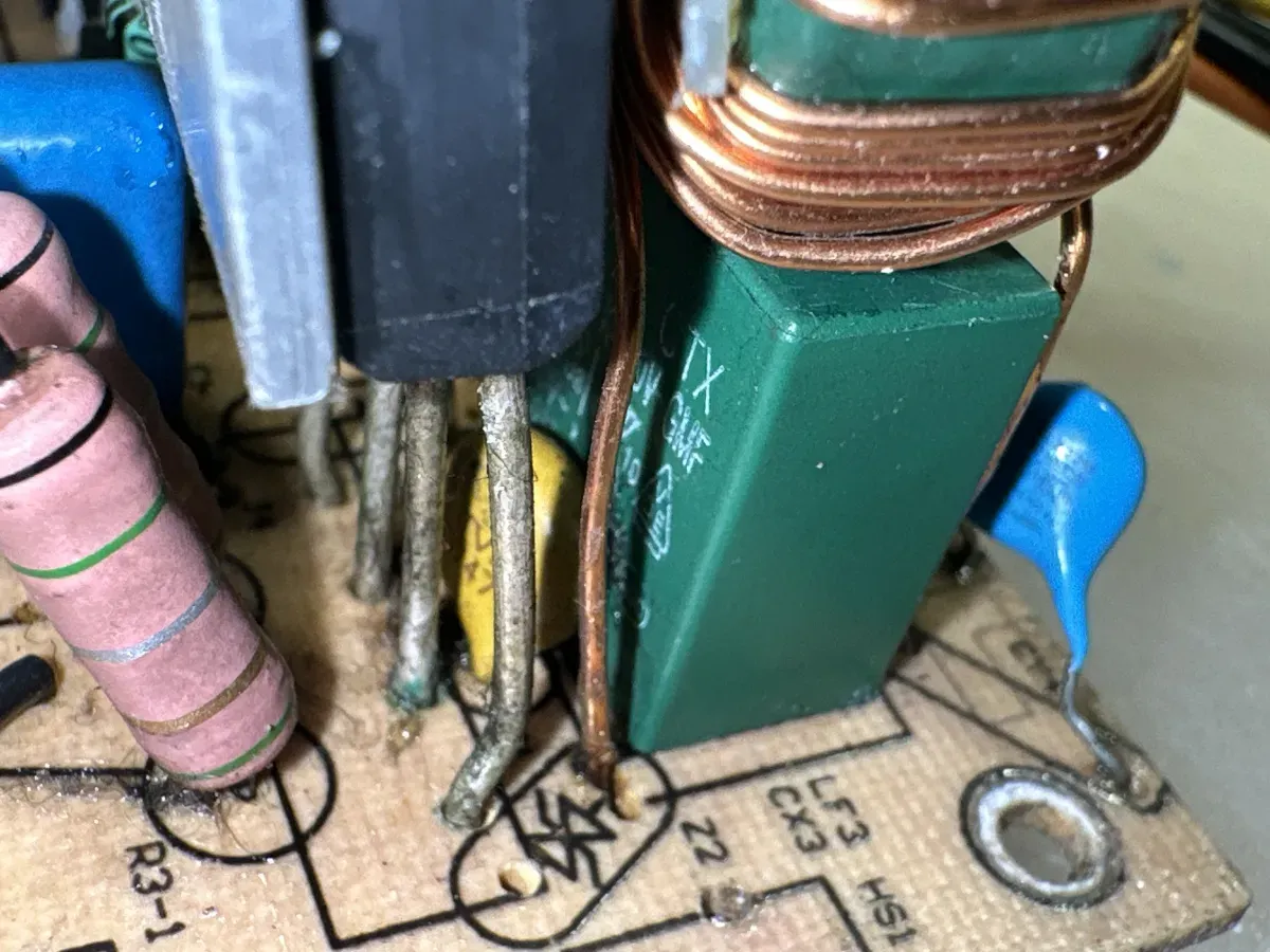
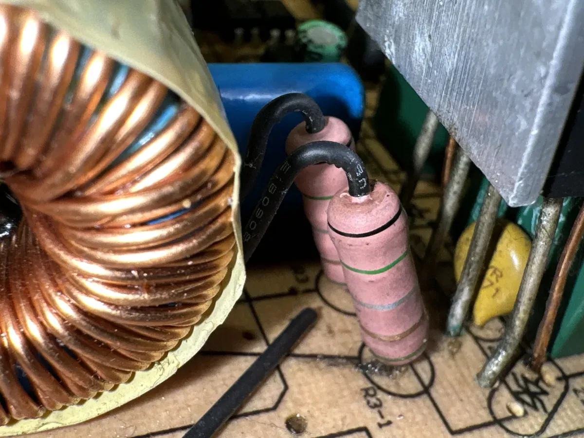
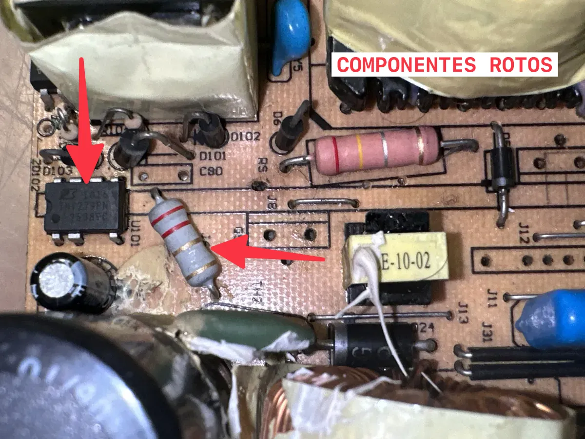
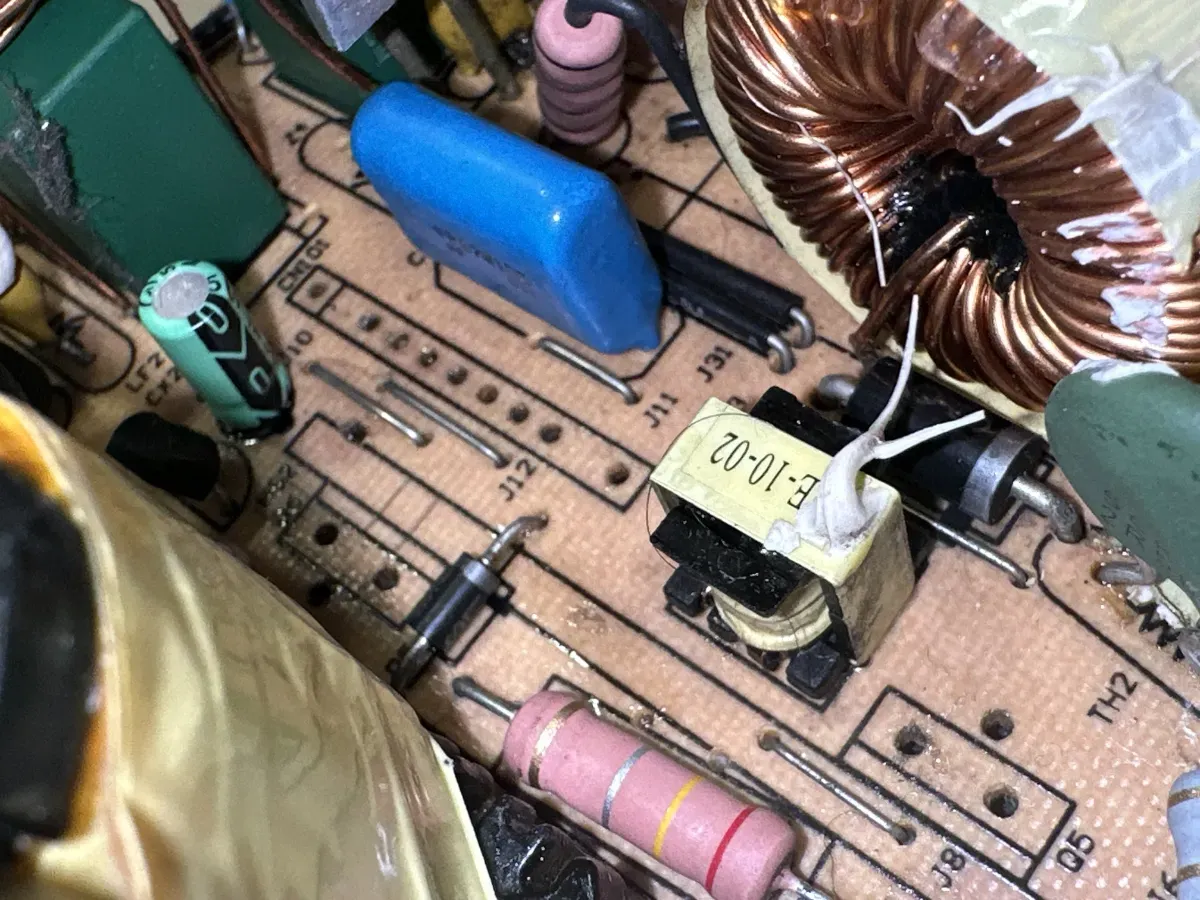
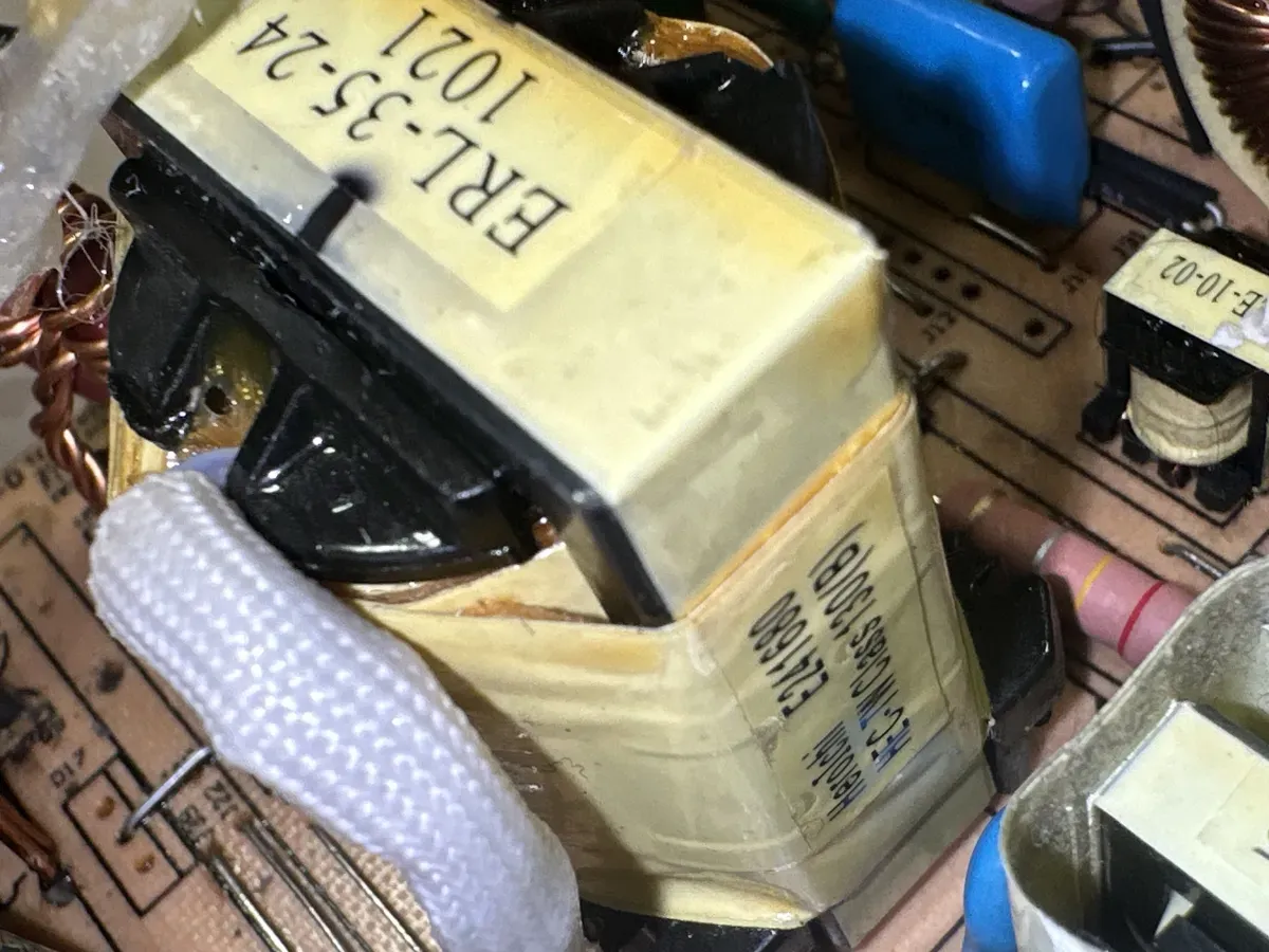

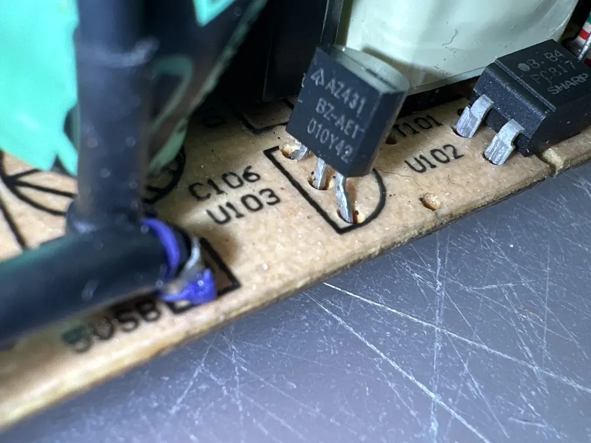
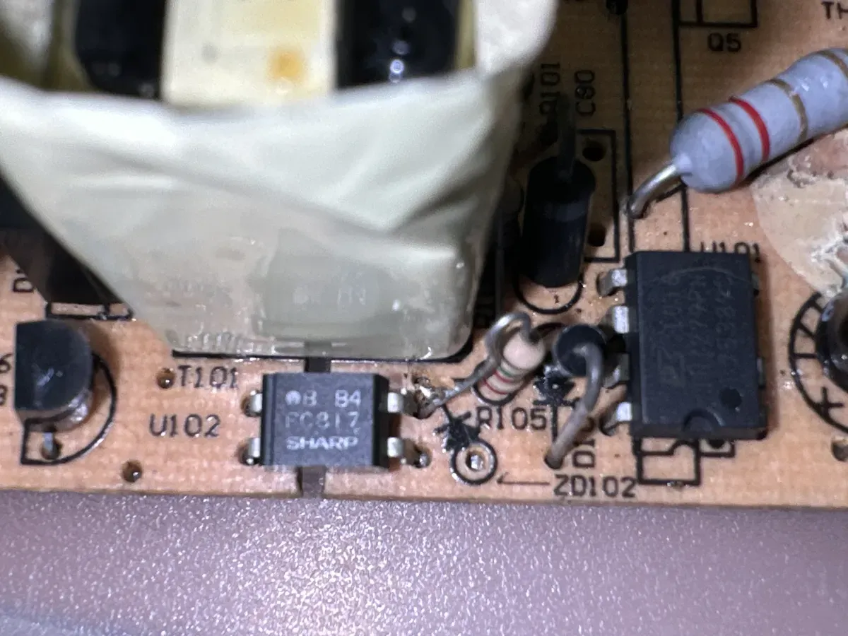
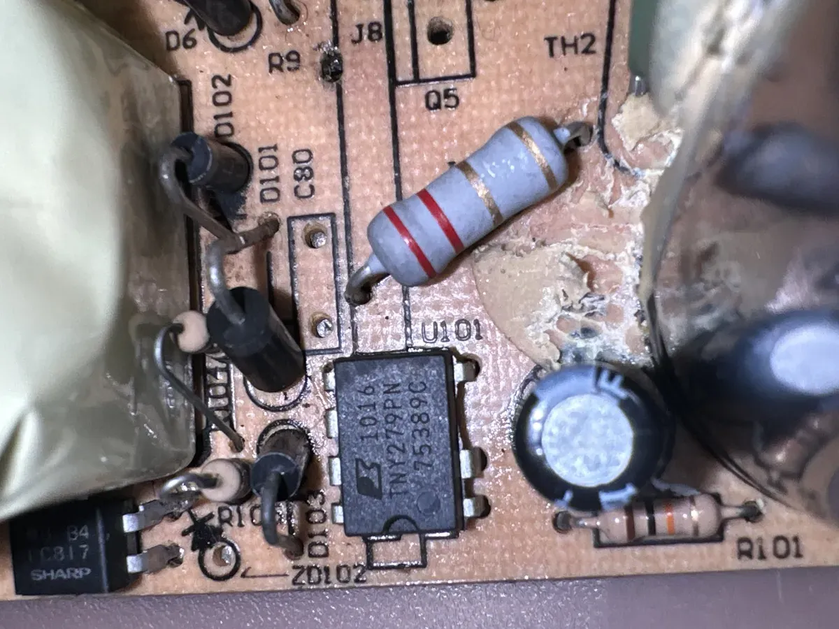
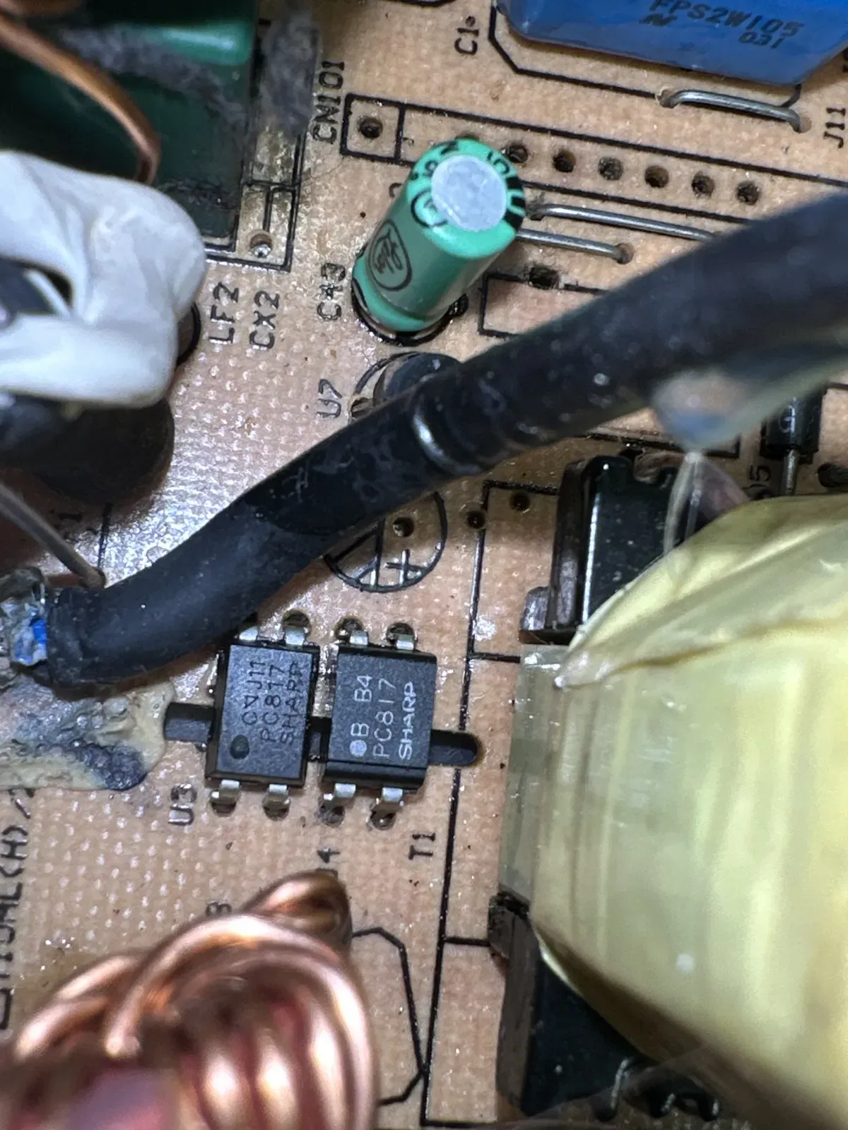
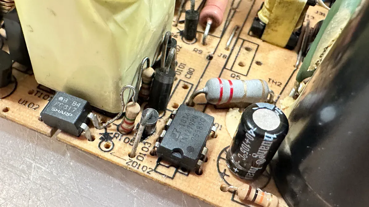
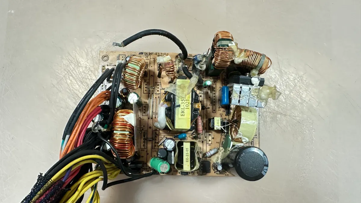
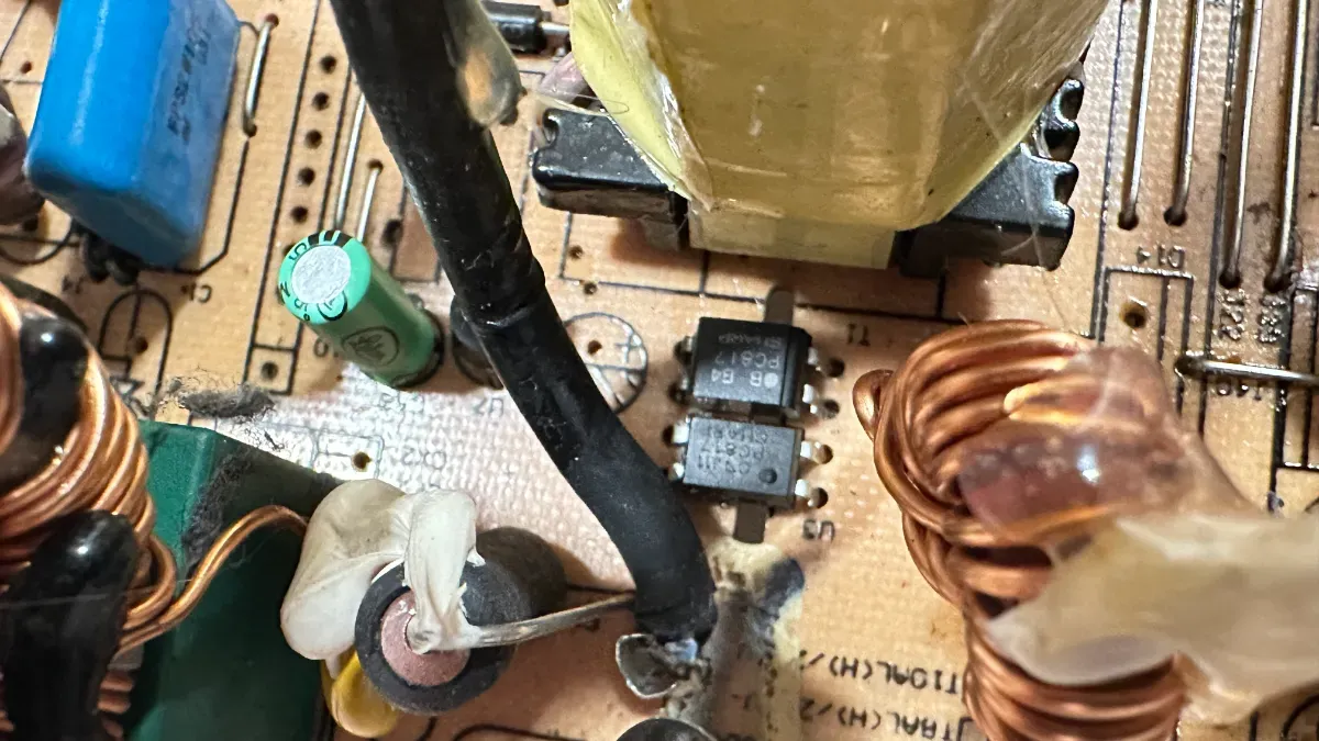
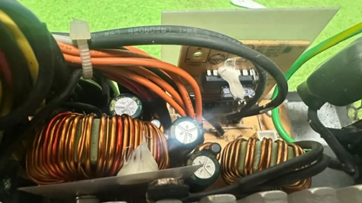
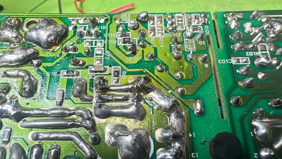
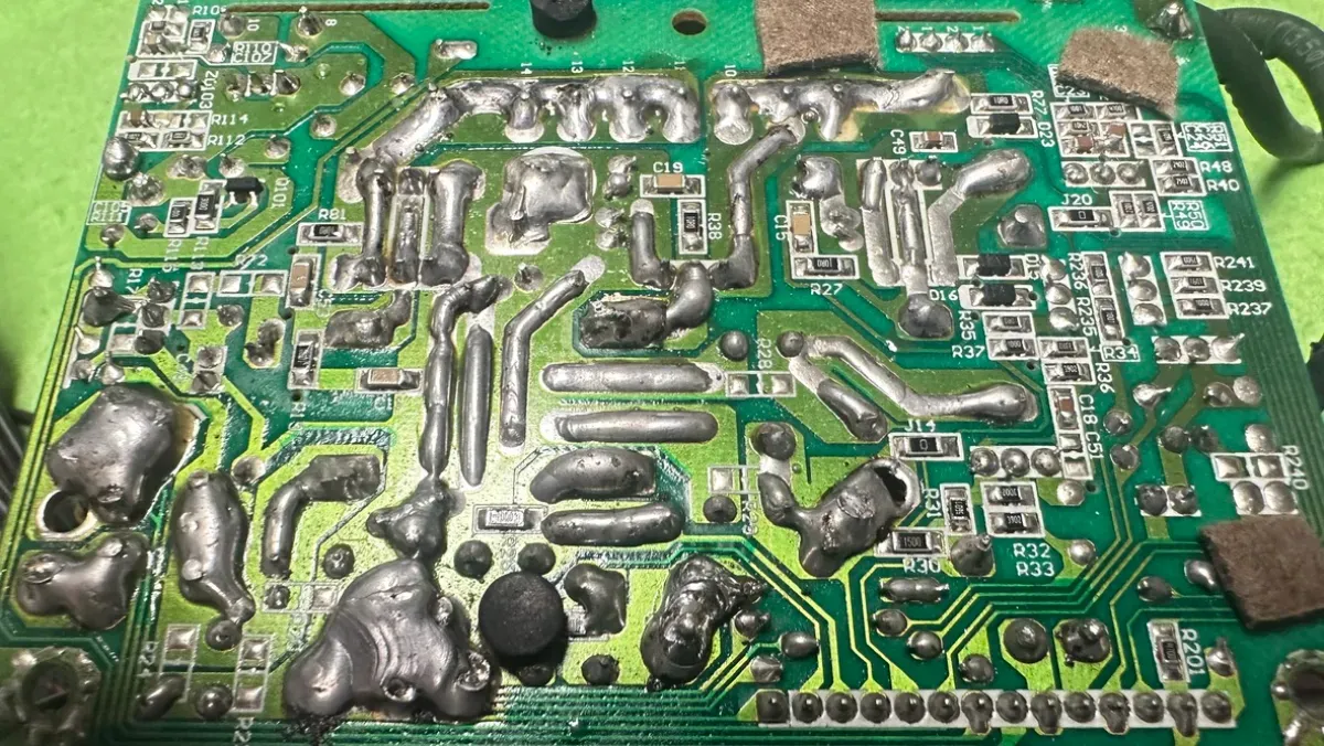
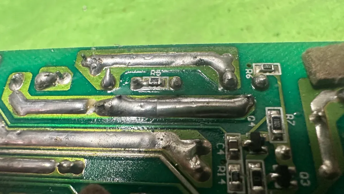
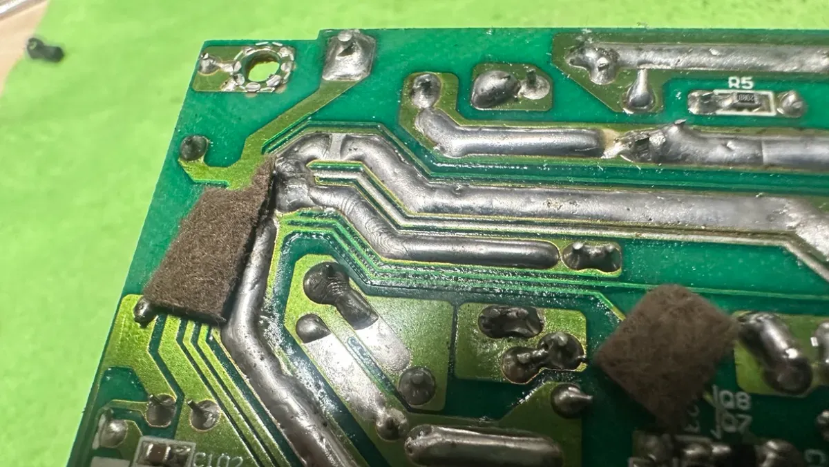
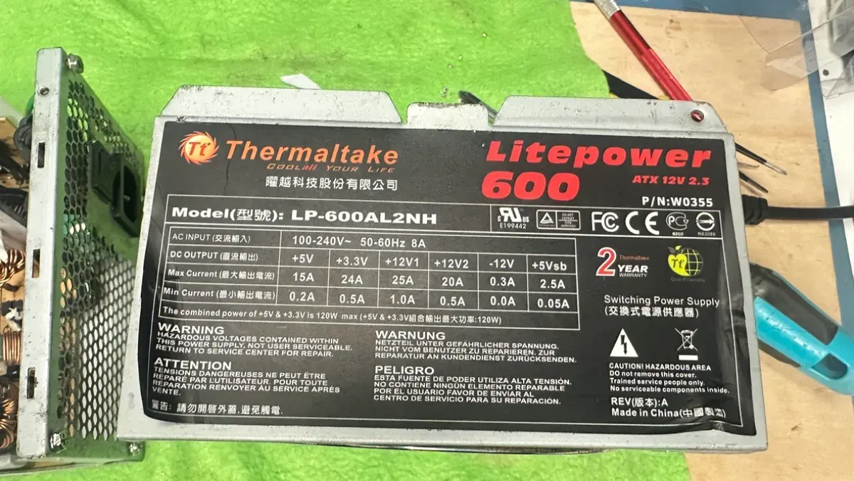
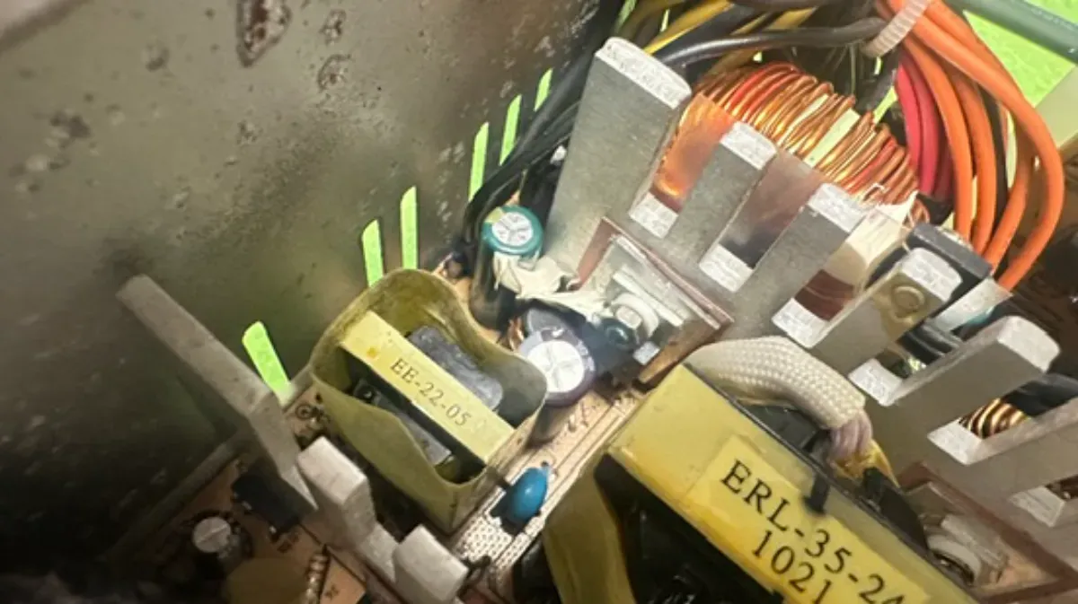
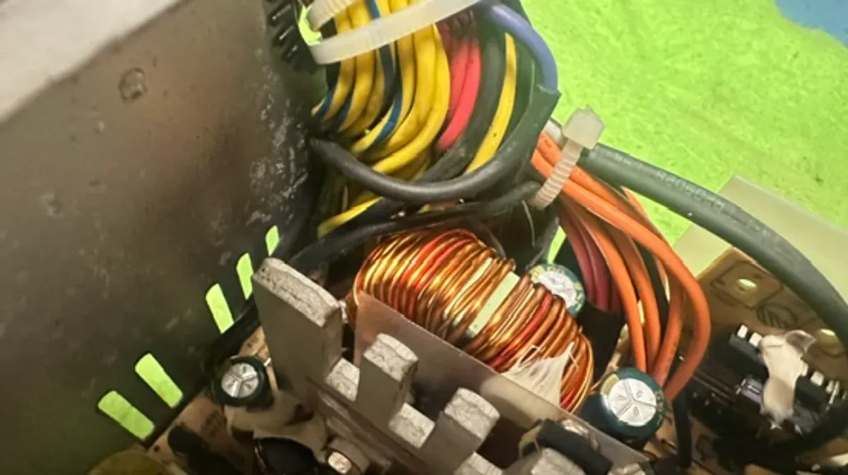
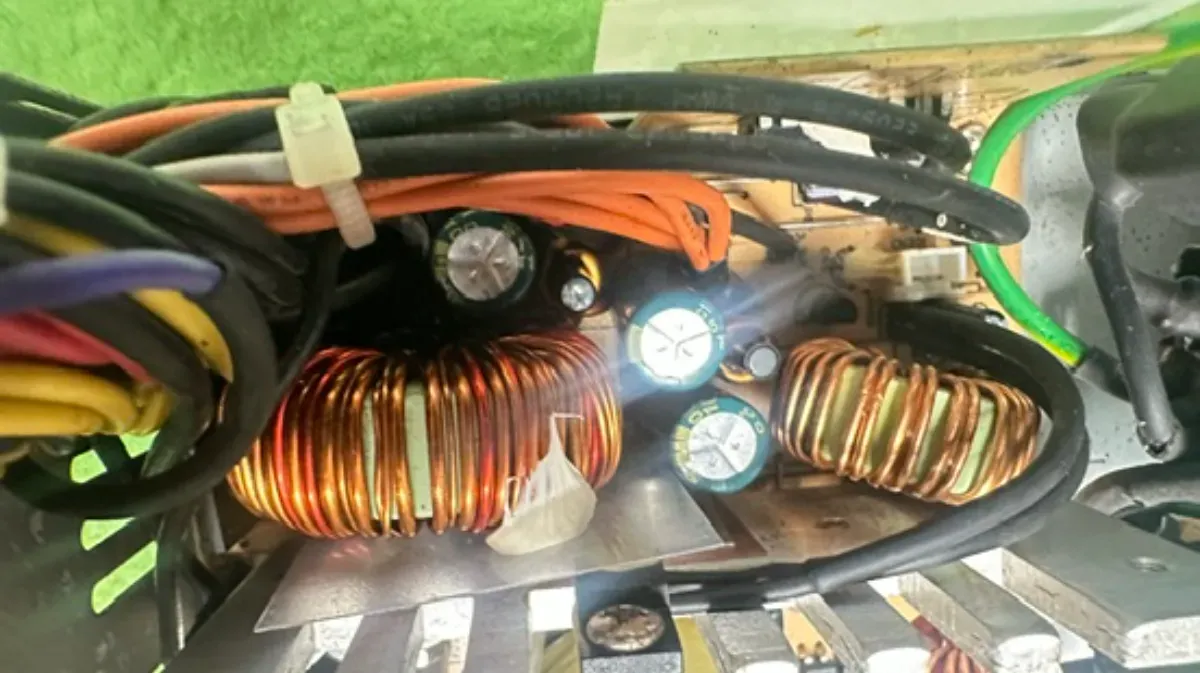
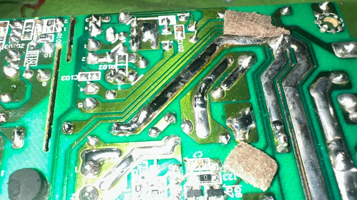
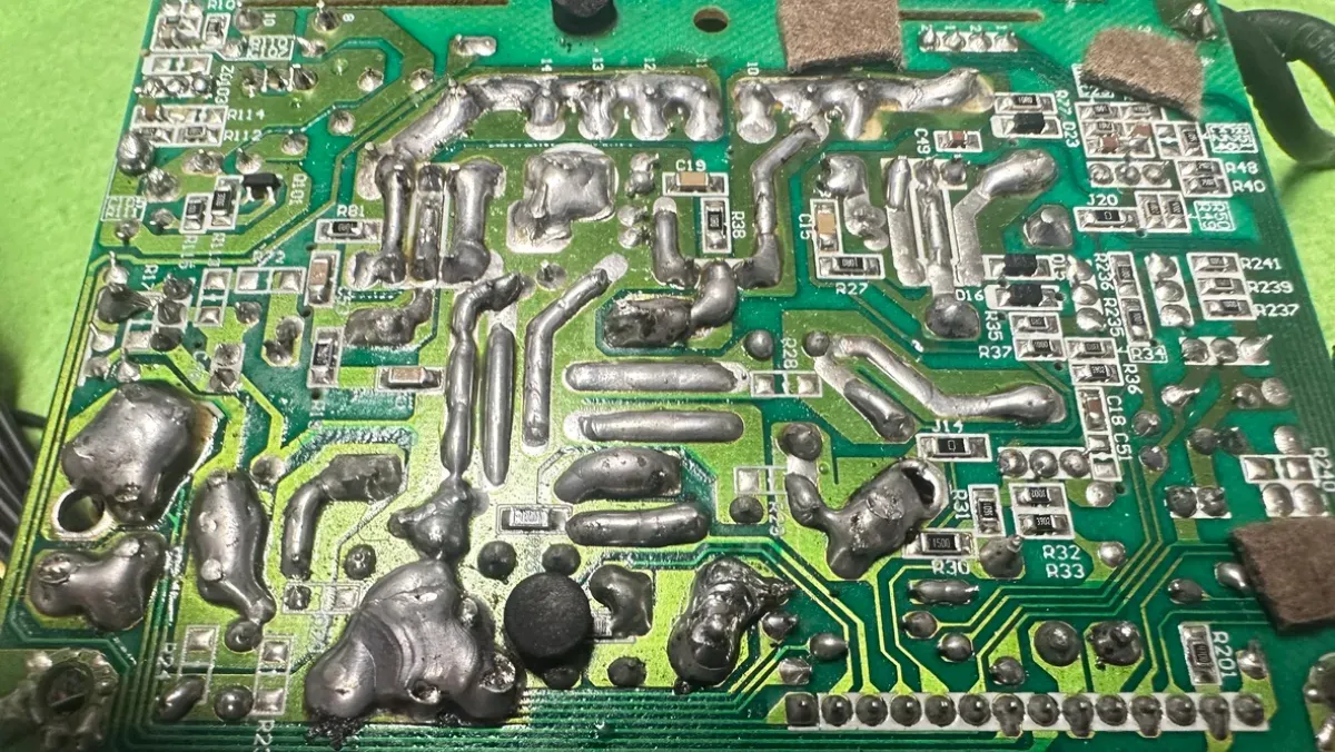
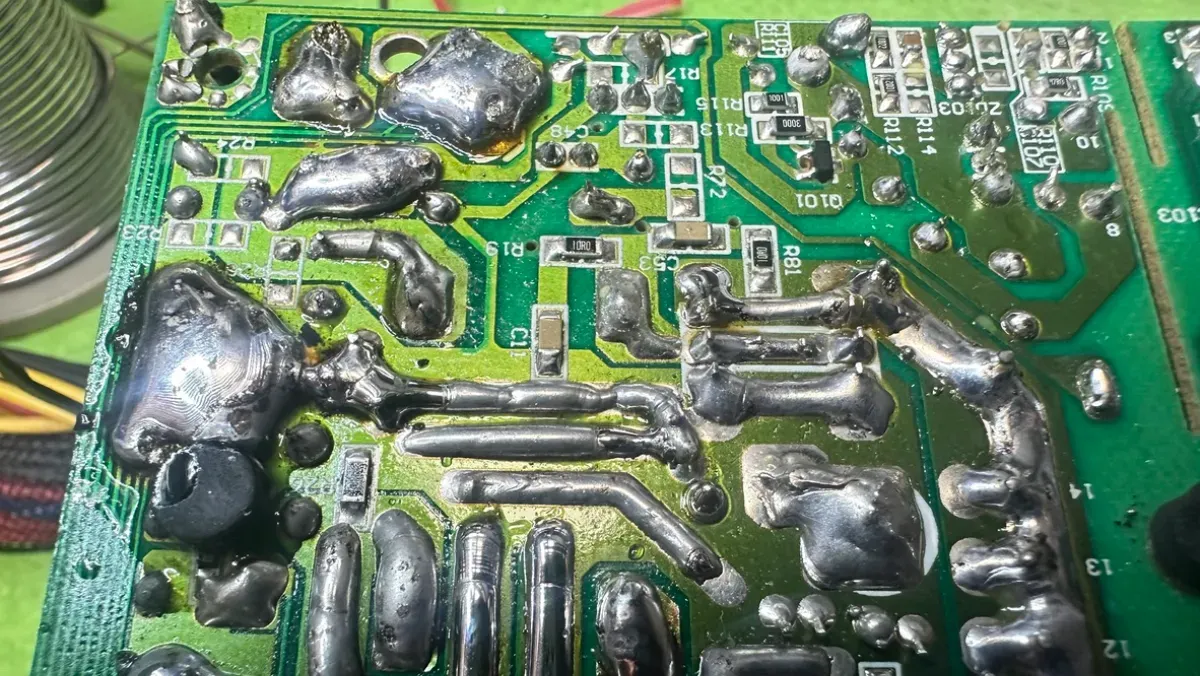
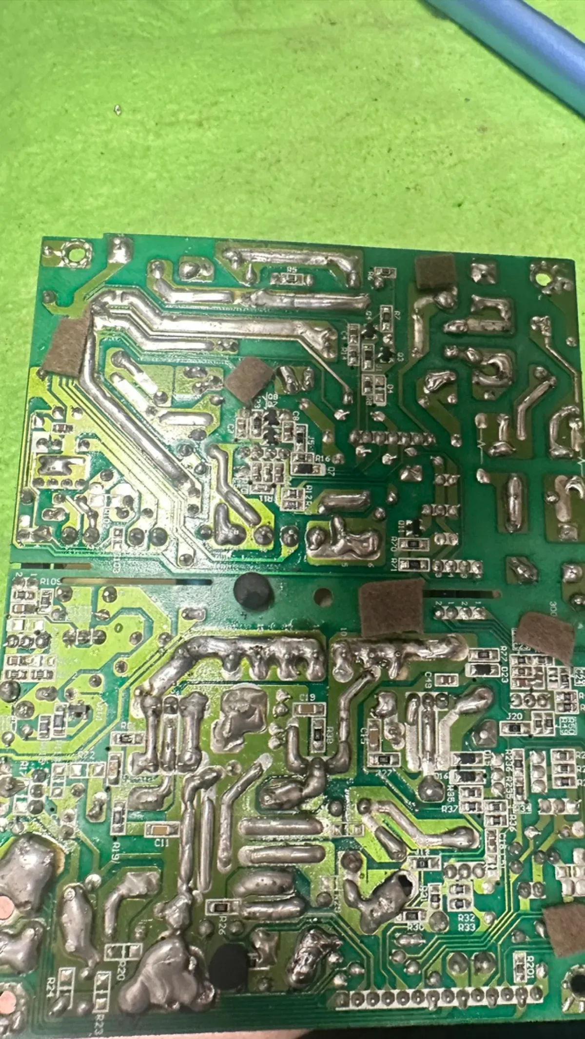
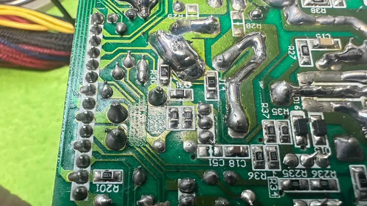
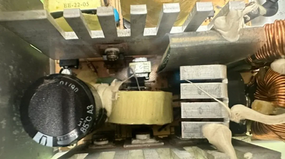
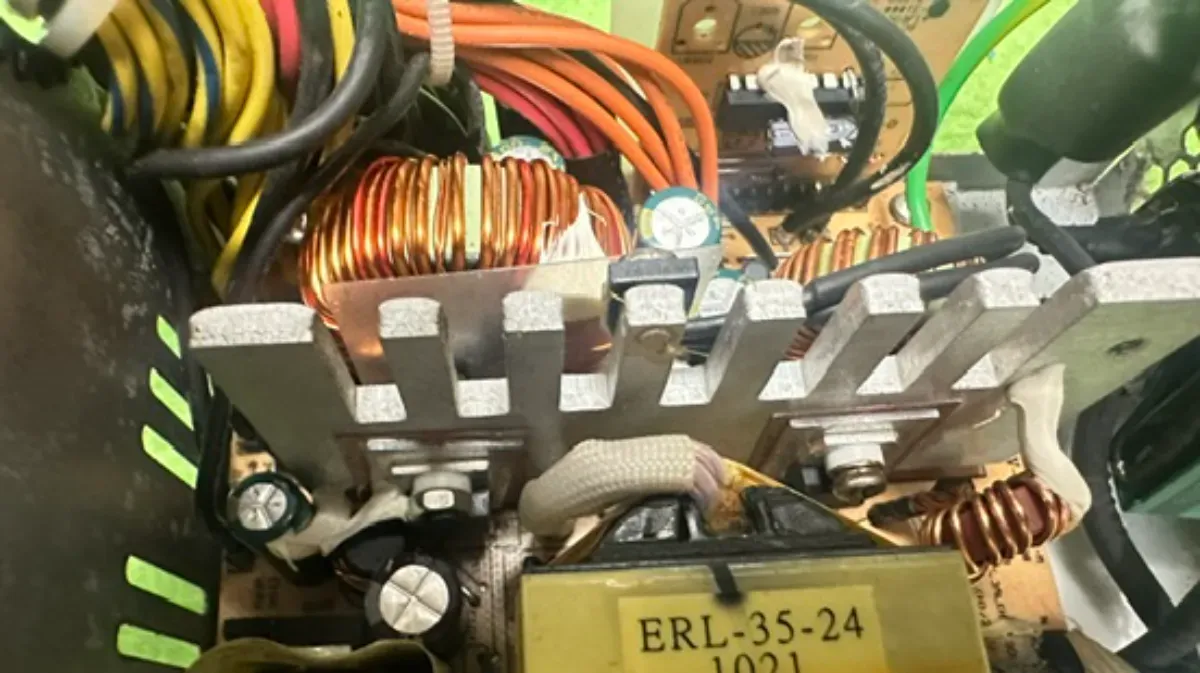
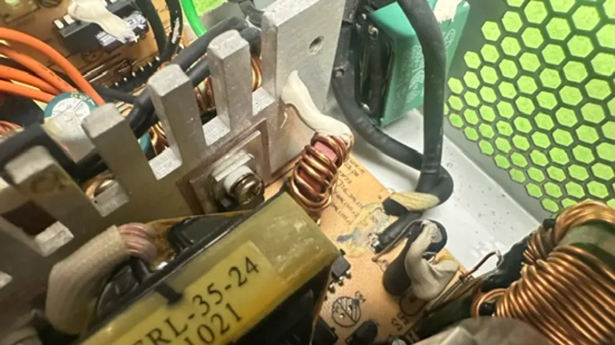
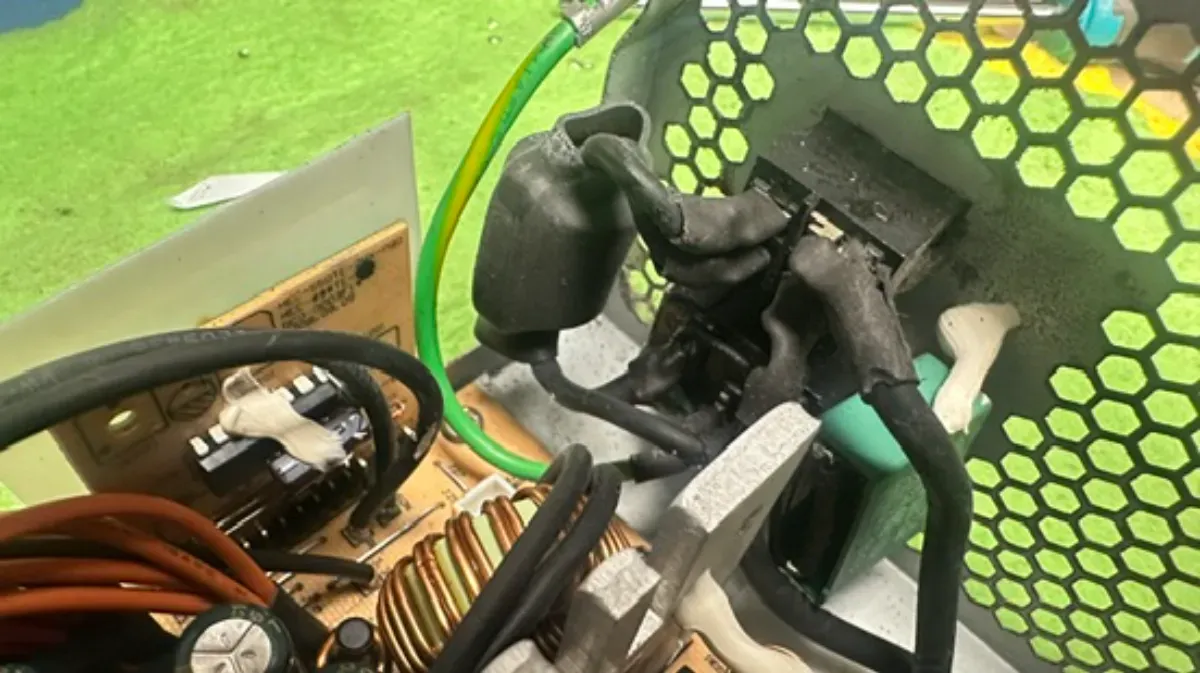
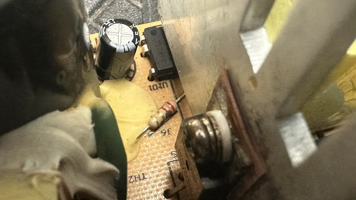
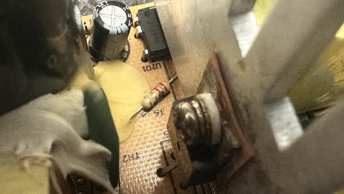
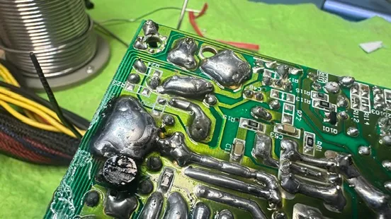
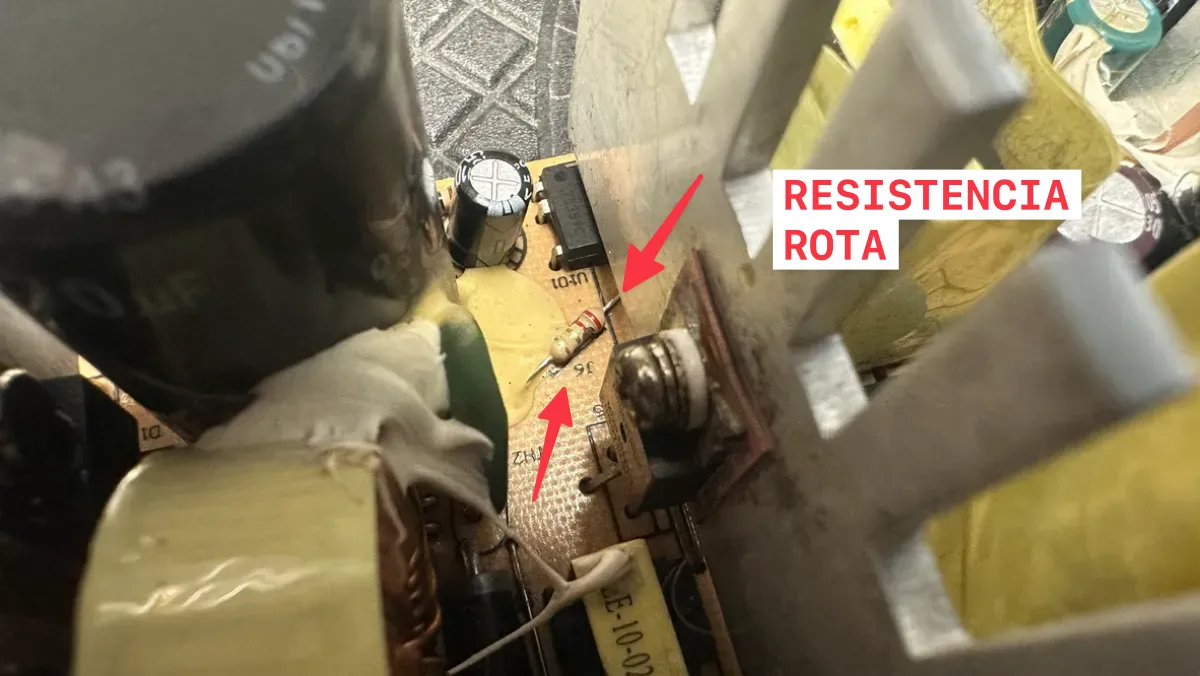
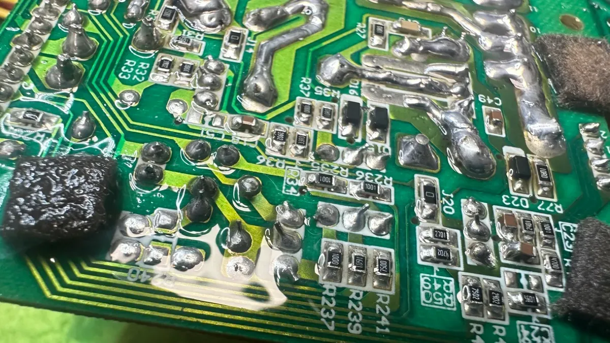
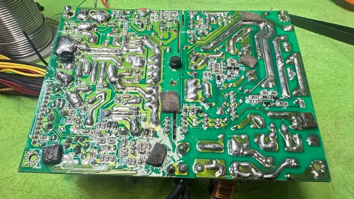
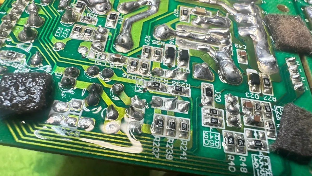
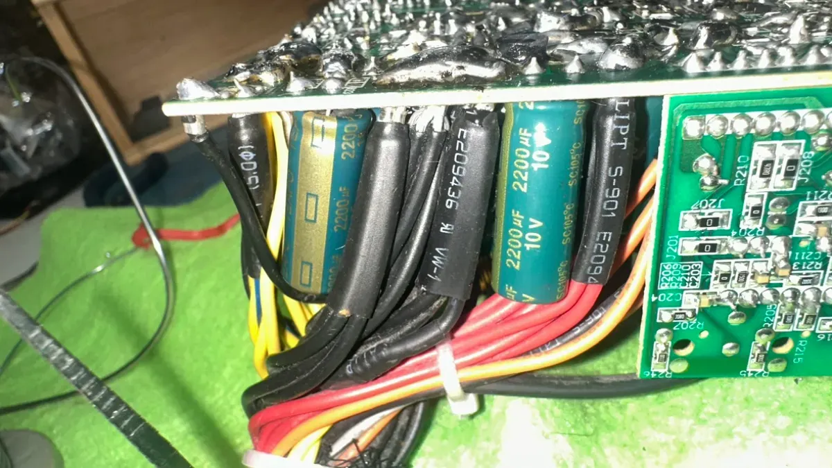
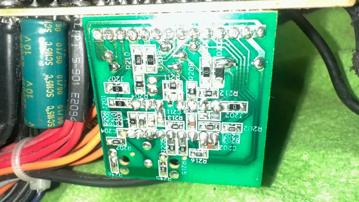
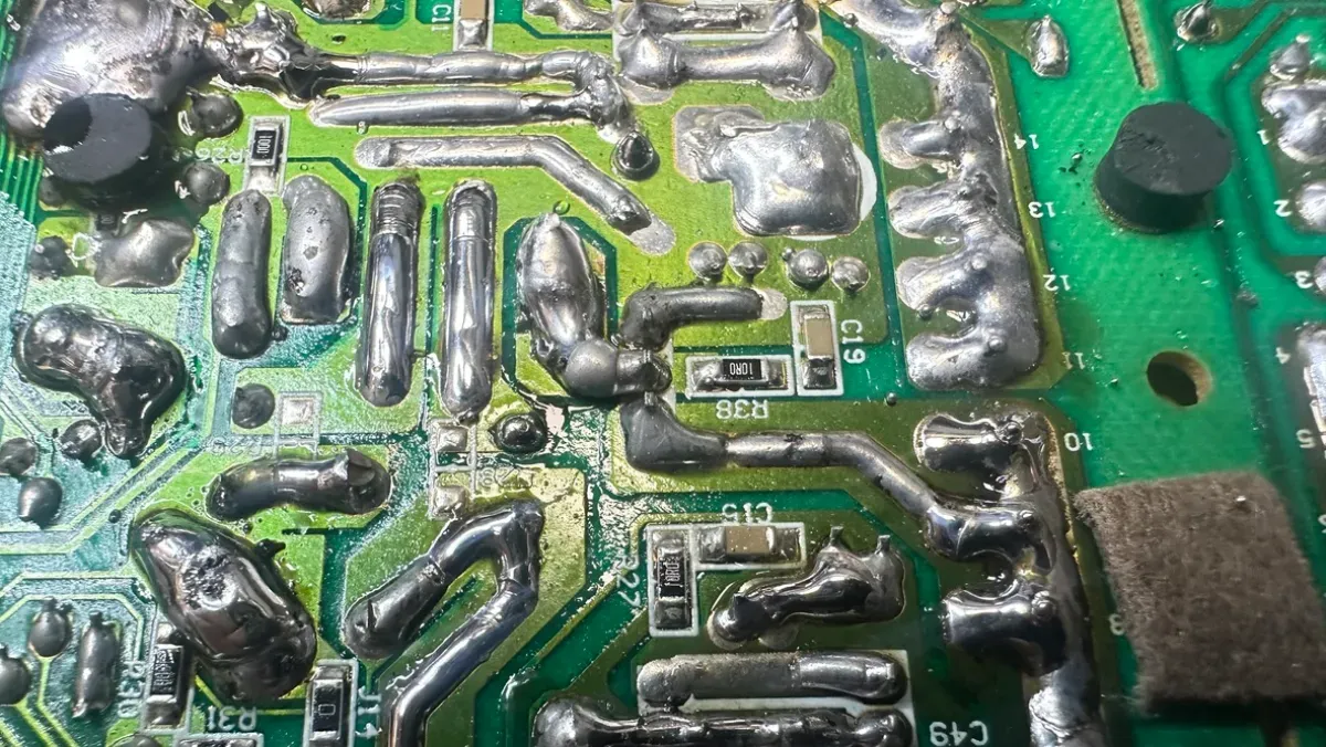
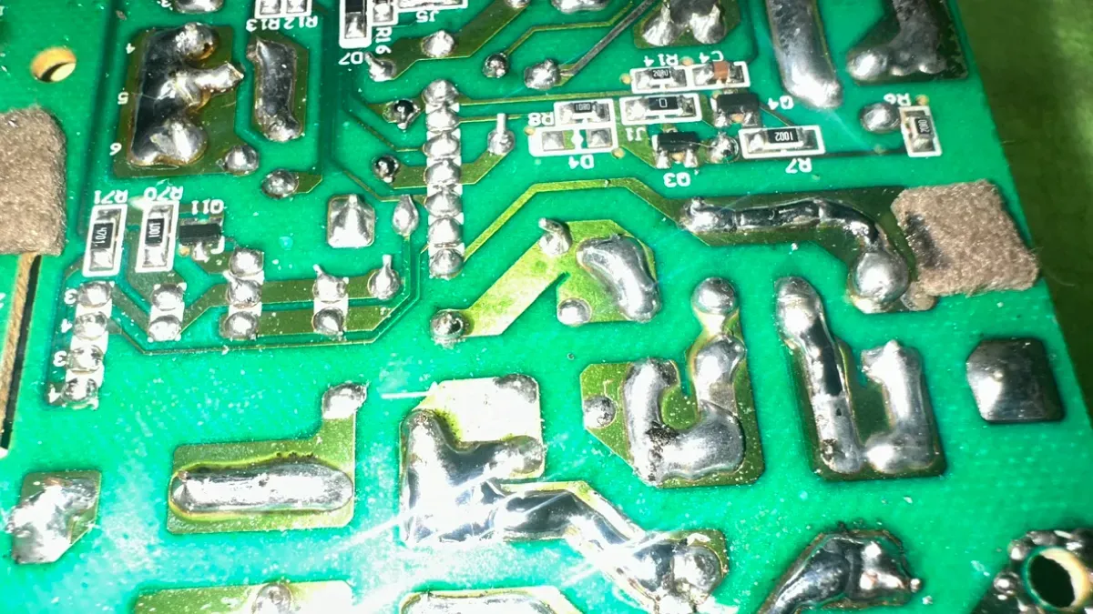
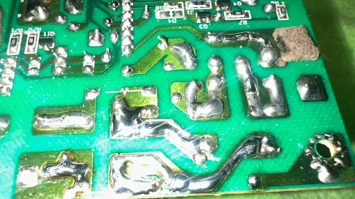
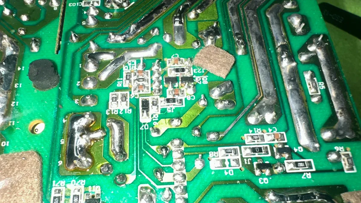
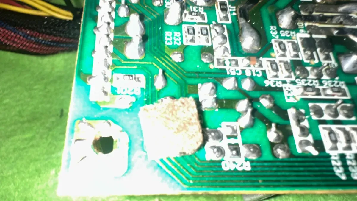
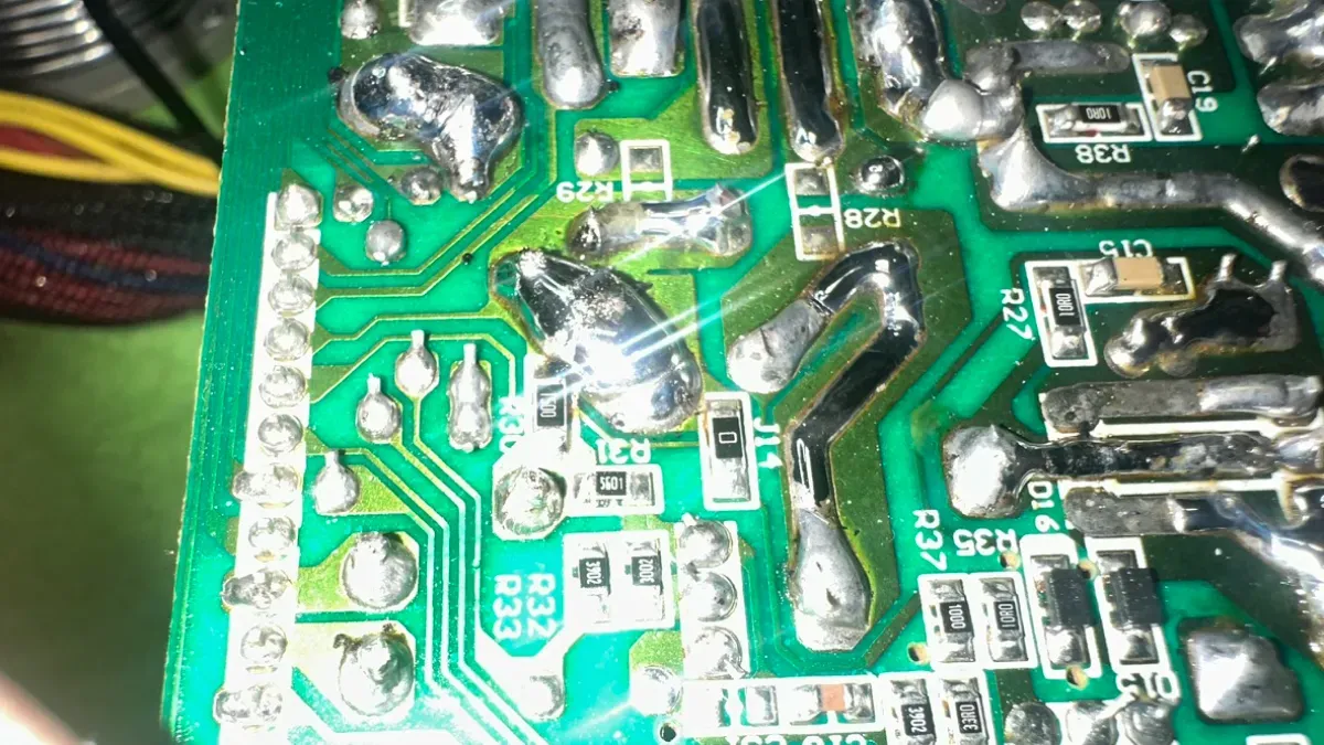
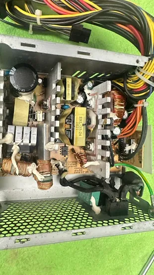
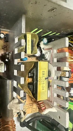
REPUESTO PEDIDO EL DIA 02-11-2026 FUENTE ESTA ENCIMA DE LA PUERTA HAY QUE PONER EL IC Y REVISAR POSIBLES CORTOS HAY QUE BARNIZAR NO ENCHUFAR HAY QUE PONER EL TERMICO AL DISPADOR
PONER TNY279 PN